 ALLPCB


In today's fast-paced electronics industry, precision and efficiency are non-negotiable. Printed Circuit Boards (PCBs) form the backbone of every electronic device, from smartphones to medical equipment, and their fabrication demands cutting-edge technology to keep up with shrinking sizes and rising complexity. Enter Laser Direct Imaging (LDI)—a game-changing innovation that's transforming how we design and produce PCBs. Unlike traditional methods that rely on physical masks and UV light, LDI uses a computer-controlled laser to directly etch circuit patterns with unmatched accuracy. For engineers, this means tighter tolerances, faster prototyping, and the ability to tackle high-density designs head-on.
Why does this matter? As devices get smaller and more powerful, the need for fine traces—sometimes as narrow as 25 micrometers (µm)—and precise alignments pushes conventional photolithography to its limits. LDI steps in to meet these challenges, offering a streamlined, mask-free process that's redefining PCB manufacturing. In this blog, we'll dive into how LDI works, its advantages over older techniques, and why it's becoming the go-to solution for modern electronics. Let's explore the technology that's driving the future of PCB fabrication.
What is Laser Direct Imaging (LDI)?
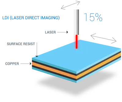
Laser Direct Imaging is an advanced PCB fabrication technique that replaces the traditional photolithography process with a digital, laser-based approach. Instead of using physical photomasks and broad UV light exposure, LDI employs a highly focused laser beam to directly 'write' circuit patterns onto a photoresist-coated PCB substrate. Controlled by a computer system loaded with design files (like Gerber data), the laser scans the board in a raster pattern, selectively exposing the photoresist to define traces, vias, and other features.
The process starts with a PCB coated in a photosensitive resist. The laser, typically operating in the ultraviolet (UV) spectrum, triggers a chemical reaction in the resist, hardening the exposed areas. After exposure, the unhardened resist is washed away, and the board is etched to remove unwanted copper, leaving the final circuit pattern. This maskless method eliminates multiple steps and variables tied to traditional techniques, making it faster and more precise.
How LDI Differs from Traditional Photolithography
To appreciate LDI's impact, let's compare it to the conventional photolithography process engineers have relied on for decades. Traditional methods begin with creating a photomask—a physical template of the circuit pattern made from film or glass. This mask is aligned over a photoresist-coated PCB, and UV light is shone through it to expose the resist. After development and etching, the pattern emerges on the board.
While effective, this approach has limitations. Photomasks take time to produce—sometimes hours or days—and any design change requires a new mask, driving up costs and delays. Alignment errors can creep in, especially with multilayer boards, where tolerances as tight as ±10 µm are critical. Environmental factors like temperature and humidity can also distort the mask, leading to defects like light diffraction or misalignment, which compromise trace widths (e.g., variations of 15-20 µm).
LDI flips this on its head. By using a digital file and a laser, it skips the mask entirely. The laser's precision—down to a spot size of 25 µm or less—ensures consistent trace widths and spacing, even for high-density interconnect (HDI) boards with lines as fine as 50/50 µm (track/space). Registration accuracy improves to within ±5 µm, thanks to real-time optical adjustments that compensate for board warpage or stretching. For engineers, this means fewer reworks and higher yields.
Suggested Reading: Laser Direct Imaging (LDI) vs. Traditional Photolithography: Choosing the Right PCB Imaging Method
Key Advantages of LDI in PCB Fabrication
LDI isn't just a tweak to the old process—it's a leap forward. Here's why it's revolutionizing PCB manufacturing:
1. Unmatched Precision and Resolution
LDI's laser can achieve sub-micron accuracy, crafting traces and spaces as small as 25 µm. This is critical for HDI boards, where microvias (50-150 µm in diameter) and dense layouts are standard. Compared to photolithography's 15-20 µm variation, LDI keeps deviations below 5 µm, ensuring signal integrity for high-speed applications like 5G devices running at gigabit data rates.
2. Faster Turnaround Times
Without photomasks, LDI slashes production time. Design changes? Just update the Gerber file—no need to fabricate a new mask. This agility is a boon for prototyping, where engineers might iterate designs multiple times. Automated laser scanning also speeds up exposure, processing up to 150 panels per hour in some systems, compared to slower mask-based setups.
3. Cost Efficiency for Small Runs
Photomasks carry upfront costs and ongoing expenses for storage and maintenance. LDI eliminates these, making it ideal for low-volume production or quick-turn projects. While the initial investment in LDI equipment is higher, the savings on masks and reduced scrap rates balance the equation over time.
4. Environmental Benefits
Traditional photolithography uses chemicals to develop masks and relies on energy-intensive UV exposure. LDI cuts chemical usage with its dry laser process and compact systems, aligning with sustainable manufacturing goals—a win for engineers prioritizing eco-friendly solutions.
5. Flexibility for Complex Designs
HDI, flex, and rigid-flex PCBs demand intricate patterns and tight tolerances. LDI's dynamic imaging adapts to substrate variations, ensuring uniform exposure even on uneven surfaces. This flexibility supports innovations like multilayer boards with 10+ layers or flexible circuits for wearables.
Applications of LDI in Modern Electronics
LDI's capabilities shine in industries pushing the boundaries of size, speed, and functionality. Here are some key areas where it's making a difference:
High-Density Interconnect (HDI) PCBs
HDI boards, with their dense wiring and microvias, power compact devices like smartphones and IoT sensors. LDI's ability to form vias as small as 25 µm and maintain ±15 µm positioning accuracy ensures reliable layer-to-layer connections, critical for signal performance at high frequencies (e.g., 5 GHz for 5G networks).
Flexible and Rigid-Flex PCBs
Wearables and automotive electronics often use flexible circuits that stretch or shrink during processing. LDI's optical algorithms adjust patterns in real-time, maintaining registration across layers—vital for double-sided or multilayer flex designs.
5G and High-Speed Applications
As data rates climb, trace geometry affects signal propagation. LDI's cleaner, rectangular trace profiles (versus photolithography's trapezoidal shapes) reduce skin effect losses at gigabit speeds, boosting performance for 5G infrastructure and servers.
Medical Devices
Miniaturized implants and diagnostic tools rely on tiny, precise PCBs. LDI delivers the fine features and consistency needed for these life-critical applications, where a trace width deviation of even 10 µm could disrupt functionality.
Challenges and Considerations with LDI
LDI isn't without hurdles. The upfront cost of equipment—often hundreds of thousands of dollars—can be a barrier for smaller manufacturers. Operating lasers also consumes more power than traditional UV systems, raising energy costs. For high-volume production, photolithography might still edge out LDI in cost-effectiveness due to economies of scale with masks.
Additionally, LDI requires skilled operators to manage its complex systems and maintain calibration. Substrate flatness matters too; excessive warpage can challenge even LDI's adaptive imaging, potentially affecting yields. Engineers must weigh these factors against their project's needs—precision versus budget, speed versus scale.
The Future of LDI in PCB Manufacturing
LDI is poised to grow as electronics evolve. With microvia sizes shrinking below 50 µm and trace widths approaching 15 µm, LDI's precision will only become more essential. Multi-wavelength laser systems, combining UV, blue, and green lasers, are emerging to optimize exposure for diverse resists and substrates. Real-time adaptive imaging, adjusting laser parameters on the fly, promises even tighter control over complex designs.
Industry 4.0 integration is another frontier. LDI systems linked to smart factories can streamline workflows, using data analytics to predict and correct defects before they occur. As demand for HDI, flex, and high-speed PCBs surges—projected to grow the global LDI market to $1.15 billion by 2033 at a 3.7% CAGR—LDI will remain at the forefront of PCB innovation.
How ALLPCB Leverages LDI for Engineers
For engineers navigating tight deadlines and complex designs, partnering with a manufacturer that harnesses LDI can be a game-changer. At ALLPCB, we integrate this technology into our advanced manufacturing processes to deliver precision-engineered PCBs with quick-turn prototyping. Our global logistics ensure fast delivery, while our expertise in HDI and flex circuits supports your most demanding projects. Whether you're prototyping a 5G module or scaling a medical device, our LDI capabilities help you achieve high yields and reliable performance without the hassle.
Conclusion
Laser Direct Imaging is more than a trend—it's a revolution in PCB fabrication. By ditching photomasks for a digital, laser-driven process, LDI delivers the precision, speed, and flexibility engineers need to meet modern electronics' demands. From HDI boards with 25 µm traces to flex circuits for wearables, it's powering the next generation of devices with fewer defects and faster turnarounds. While challenges like cost and complexity remain, LDI's trajectory points upward, promising even greater advancements as technology evolves.
For engineers, understanding LDI means unlocking new possibilities in design and production. It's a tool that not only solves today's challenges but also paves the way for tomorrow's innovations. As we push the boundaries of what PCBs can do, LDI stands as a cornerstone of that progress—precise, efficient, and ready for the future.


