 ALLPCB


In the fast-evolving world of electronics manufacturing, ensuring high-quality solder joints on printed circuit boards (PCBs) is critical. A machine vision based solder process offers a powerful solution for inspecting and verifying solder joints with precision, while adhering to International Electrotechnical Commission (IEC) compliance standards ensures safety and reliability. This blog post explores how to implement a machine vision PCB process, focusing on IEC compliance, and dives into the role of technologies like machine learning and computer vision in enhancing solder joint quality.
If you're looking to improve your PCB manufacturing process with cutting-edge technology while meeting global standards, you're in the right place. We'll break down the essentials of machine vision for solder joints, the importance of IEC compliance, and practical steps to integrate these systems effectively.
What is a Machine Vision PCB Process?
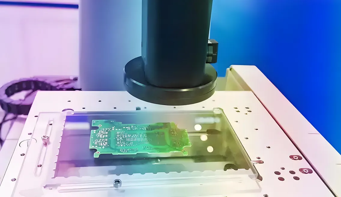
A machine vision PCB process involves using advanced imaging systems and algorithms to inspect and analyze components on a printed circuit board, with a particular focus on solder joints. Unlike manual inspection, which can be slow and prone to human error, machine vision systems use cameras, lighting, and software to detect defects such as insufficient solder, bridging, or misaligned components. This technology is essential for high-volume production lines where precision and speed are non-negotiable.
Machine vision systems capture high-resolution images of PCBs, often at multiple angles, under controlled lighting conditions. These images are then processed using specialized software to identify anomalies. When integrated with machine learning, these systems can even learn from past inspections to improve accuracy over time, making them invaluable for modern electronics manufacturing.
Why IEC Compliance Matters for Solder Processes
IEC compliance refers to adhering to standards set by the International Electrotechnical Commission, a global organization that develops guidelines for electrical and electronic technologies. For PCB manufacturing, IEC standards like IEC 61191 (for soldered electrical connections) and IEC 60068 (for environmental testing) outline requirements for solder joint reliability, safety, and performance under various conditions.
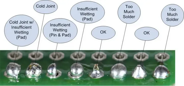
Implementing a machine vision IEC solder process ensures that your manufacturing line meets these rigorous standards. Compliance not only guarantees product quality but also builds trust with clients and reduces the risk of costly recalls or failures in the field. For instance, IEC 61191-2 specifies acceptable criteria for solder joint appearance, such as fillet shape and wetting angles, which can be precisely measured using machine vision tools.
By aligning your machine vision PCB process with IEC guidelines, you ensure that defects are caught early, and your products can withstand real-world stresses like thermal cycling or mechanical shock, as tested under IEC 60068-2-14 (thermal shock testing).
Benefits of Using Machine Vision for PCB Solder Joints
Integrating machine vision for inspecting PCB solder joints offers numerous advantages over traditional methods. Here are some key benefits:
- High Accuracy: Machine vision systems can detect defects as small as 0.1 mm, far surpassing human capabilities. This precision is crucial for identifying micro-cracks or insufficient solder that could lead to failures.
- Speed: These systems can inspect hundreds of solder joints per minute, keeping up with high-speed production lines.
- Consistency: Unlike human inspectors, machine vision doesn’t suffer from fatigue, ensuring consistent results across shifts.
- Data Collection: Machine vision systems log inspection data, allowing for traceability and process optimization. For example, if a recurring defect is detected at a specific stage, adjustments can be made to prevent future issues.
By focusing on PCB solder joints with machine vision, manufacturers can achieve near-zero defect rates, aligning with the principles of Industry 4.0 and smart manufacturing.
Role of Machine Learning in Solder Joint Inspection
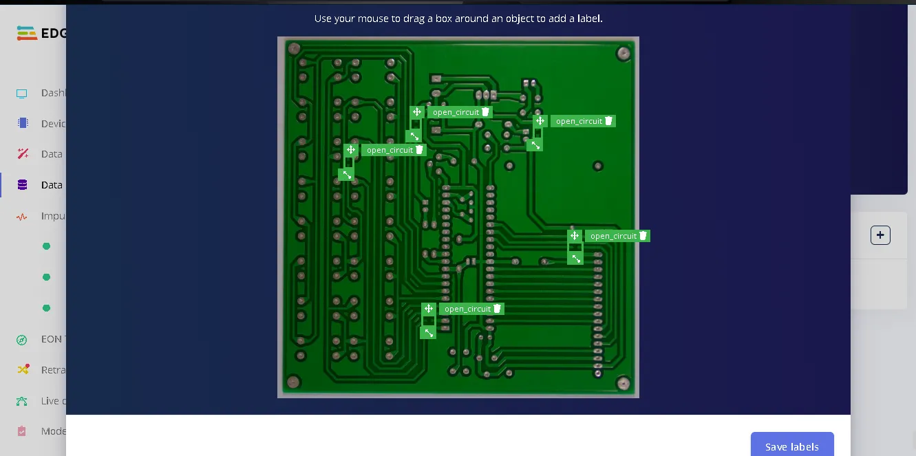
Machine learning solder joints methods have revolutionized the way defects are detected and classified. Traditional machine vision systems rely on predefined rules to identify issues, but machine learning takes this a step further by enabling systems to adapt and improve over time.
For instance, a machine learning algorithm can be trained on thousands of images of solder joints, both defective and acceptable, to recognize patterns that indicate problems. Convolutional Neural Networks (CNNs), a type of deep learning model, are particularly effective for image-based tasks like this. Studies have shown that CNN-based systems can achieve defect detection accuracy rates above 95%, even with complex defects like solder voids or incomplete wetting.
In a real-world scenario, a machine learning model might analyze X-ray images of solder joints to detect internal defects that are invisible to the naked eye. This capability is especially important for ball grid array (BGA) components, where solder joints are hidden beneath the chip. By continuously learning from new data, these systems become more adept at identifying subtle or rare defects, reducing false positives and improving overall efficiency.
Computer Vision Techniques for Solder Joints
Computer vision solder joints inspection relies on a combination of hardware and software to achieve reliable results. Here are some common techniques used in the industry:
- Image Acquisition: High-resolution cameras, often with resolutions of 5 megapixels or higher, capture detailed images of solder joints. Specialized lighting, such as coaxial or ring lights, minimizes shadows and enhances contrast.
- Image Preprocessing: Algorithms adjust brightness, contrast, and noise levels to ensure clear images for analysis. For example, a Gaussian blur filter might be applied to reduce noise without losing critical details.
- Feature Extraction: Key characteristics of solder joints, such as fillet shape, size, and surface texture, are extracted for evaluation. Edge detection algorithms like the Canny method can identify boundaries of solder fillets with precision.
- Defect Classification: Using predefined criteria or machine learning models, the system classifies joints as acceptable or defective. For instance, a joint with a wetting angle greater than 90 degrees might be flagged as non-compliant with IEC standards.
These computer vision techniques, when paired with IEC compliance guidelines, ensure that every solder joint meets stringent quality requirements, minimizing the risk of field failures.
Steps to Implement a Machine Vision Based Solder Process with IEC Compliance
Implementing a machine vision PCB process that aligns with IEC standards requires careful planning and execution. Below are the key steps to follow:
1. Define Inspection Requirements Based on IEC Standards
Start by identifying the specific IEC standards relevant to your products, such as IEC 61191 for soldered connections. Determine the acceptable criteria for solder joint appearance, including fillet height (typically 0.5 mm to 1.5 mm for surface-mount components) and wetting angles (ideally between 0 and 90 degrees). These parameters will guide your machine vision setup.
2. Select the Right Hardware
Choose high-quality cameras and lighting systems suited for PCB inspection. For example, a 12-megapixel camera with a telecentric lens can provide distortion-free images of small components. Ensure that the hardware can operate in your production environment, considering factors like temperature and vibration.
3. Develop or Integrate Software Solutions
Opt for machine vision software that supports both rule-based and machine learning approaches. If using machine learning solder joints methods, prepare a dataset of labeled images (e.g., 10,000 images with 70% good and 30% defective joints) to train your model. Ensure the software can generate reports for IEC compliance audits.
4. Calibrate the System for Accuracy
Calibrate your machine vision system to detect defects within the tolerances specified by IEC standards. For instance, if IEC 61191-2 requires a minimum solder fillet height of 0.7 mm, ensure the system can measure this with an error margin of less than 0.05 mm.
5. Test and Validate the Process
Run pilot tests on a small batch of PCBs to validate the system’s performance. Compare the machine vision results with manual inspections or X-ray imaging to confirm accuracy. Adjust thresholds and algorithms as needed to minimize false positives and negatives.
6. Document and Train for Compliance
Maintain detailed documentation of your machine vision setup, inspection criteria, and test results to demonstrate IEC compliance during audits. Train your team on operating the system and interpreting its outputs to ensure consistent quality control.
Challenges in Implementing Machine Vision for Solder Joints
While the benefits are clear, implementing a machine vision IEC solder process comes with challenges. One common issue is the high initial cost of equipment and software, which can range from $50,000 to $200,000 depending on the complexity of the system. Additionally, integrating machine vision into an existing production line may require downtime or reconfiguration, impacting short-term productivity.
Another challenge is handling the variability in PCB designs and solder joint appearances. For example, reflective surfaces or irregular component shapes can confuse standard vision algorithms, requiring custom solutions or advanced machine learning models. Finally, ensuring compliance with IEC standards demands regular updates to software and processes as standards evolve, adding to maintenance efforts.
Despite these hurdles, the long-term gains in quality and efficiency make machine vision a worthwhile investment for PCB manufacturers.
Future Trends in Machine Vision for PCB Manufacturing
The field of machine vision for PCB solder joints is rapidly advancing, driven by innovations in artificial intelligence and imaging technology. One emerging trend is the use of 3D imaging for more comprehensive inspections. Unlike 2D systems, 3D machine vision can measure the height and volume of solder fillets, providing deeper insights into joint quality.
Another trend is the integration of real-time analytics with machine vision systems. By connecting to cloud-based platforms, manufacturers can monitor inspection data across multiple facilities, identifying trends and optimizing processes on a global scale. Additionally, advancements in machine learning will continue to improve defect detection accuracy, potentially reaching 99% or higher in the coming years.
Staying ahead of these trends will ensure that your machine vision PCB process remains competitive and compliant with evolving IEC standards.
Conclusion
Implementing a machine vision based solder process with IEC compliance is a game-changer for PCB manufacturing. By leveraging technologies like computer vision and machine learning solder joints methods, manufacturers can achieve unparalleled precision and reliability in inspecting solder joints. Adhering to IEC standards ensures that products meet global safety and performance requirements, building trust with customers and reducing risks.
From selecting the right hardware to calibrating systems for accuracy, the steps outlined in this blog provide a clear roadmap for integrating machine vision into your production line. While challenges like cost and variability exist, the long-term benefits of improved quality and efficiency far outweigh the initial hurdles. As technology continues to evolve, staying updated on trends like 3D imaging and real-time analytics will keep your process at the forefront of innovation.
With a well-implemented machine vision IEC solder process, you can elevate your PCB manufacturing to new heights, ensuring every solder joint meets the highest standards of quality and compliance.


