 ALLPCB


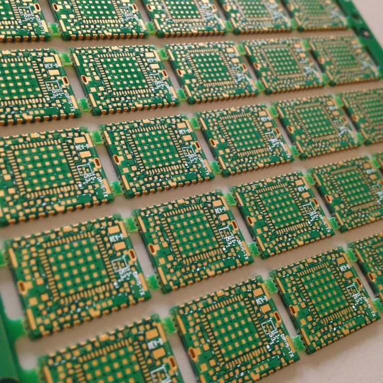
Pre-treatment is a critical step in the PCB manufacturing process, especially when it comes to plating. Mistakes during this phase can lead to plating failures, causing defects, poor adhesion, or even complete board failure. In this comprehensive guide, we’ll explore the most common errors in plating pretreatment, including issues with cleaning PCBs, degreasing PCBs, the etching process, and the use of PCB process fluids. By understanding these pitfalls and how to avoid them, you can prevent electroplating issues and ensure high-quality results for your printed circuit boards.
Why Pre-Treatment Matters in PCB Plating
Before diving into the specific mistakes, let’s understand why pre-treatment is so important. Plating is the process of depositing a metal layer, often copper, onto the PCB surface to create conductive pathways or protect the board. However, for the plating to adhere properly and function as intended, the surface must be perfectly prepared. Pre-treatment involves cleaning, degreasing, and etching the board to remove contaminants and create a suitable surface for plating. Any oversight in these steps can result in weak adhesion, uneven plating, or defects that compromise the board’s performance.
Common Mistakes in Plating Pretreatment
Let’s break down the frequent errors made during pre-treatment that often lead to plating failure. By addressing these issues, you can improve the reliability and quality of your PCB production.
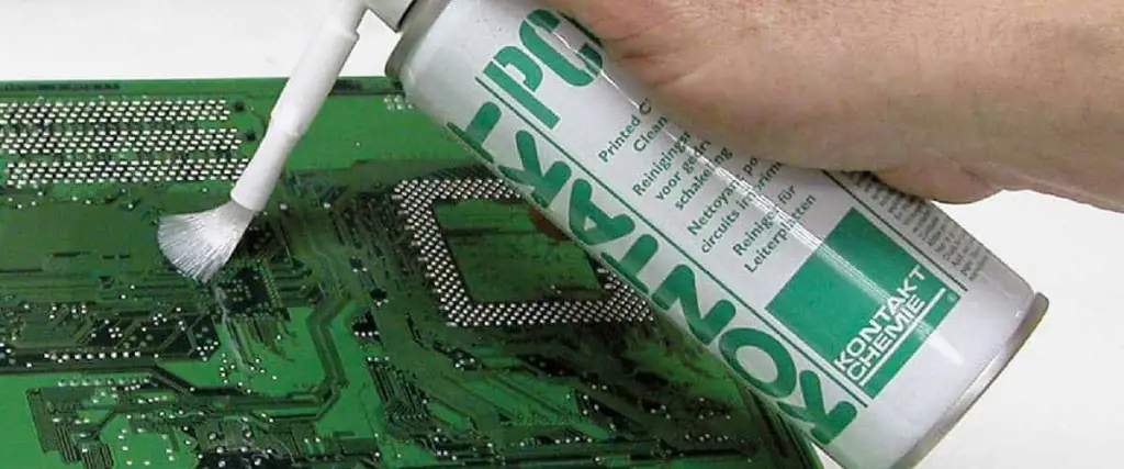
1. Inadequate Cleaning of PCBs
One of the most common mistakes in cleaning PCBs is failing to remove all contaminants from the surface before plating. Dust, fingerprints, oils, and residues from previous manufacturing steps can create barriers between the board and the plating material. This results in poor adhesion, leading to peeling or flaking of the plated layer.
To avoid this, ensure that the cleaning process uses appropriate solvents or aqueous solutions to eliminate organic and inorganic residues. For instance, a study in PCB manufacturing found that boards cleaned with isopropyl alcohol (90% or higher) showed a 30% improvement in plating adhesion compared to those cleaned with less effective methods. Additionally, using ultrasonic cleaning can enhance the removal of stubborn particles, especially in high-density boards with fine features.
Tip: Always inspect the board visually and under magnification after cleaning to confirm no residues remain. Implementing a consistent cleaning protocol can reduce plating defects by up to 25%.
2. Poor Degreasing of PCBs
Another critical error in degreasing PCBs is using ineffective or outdated degreasing agents. Grease and oils left on the surface can prevent proper etching and plating, leading to uneven metal deposition or voids in the plated layer. This is especially problematic in high-frequency boards where even small defects can affect signal integrity, sometimes increasing impedance by as much as 15% beyond acceptable limits.
Modern degreasing often involves alkaline or solvent-based solutions tailored to the specific contaminants on the board. A common oversight is skipping the rinse step after degreasing, which can leave chemical residues that interfere with subsequent processes. Ensure a thorough rinse with deionized water to achieve a clean, residue-free surface.
Tip: Test the degreasing solution’s effectiveness periodically by checking for water break-free surfaces. If water beads up on the board, it indicates grease is still present, and further degreasing is needed.
3. Incorrect Etching Process
The etching process is designed to create a micro-rough surface on the PCB for better plating adhesion. However, mistakes in this step can lead to over-etching or under-etching, both of which cause significant electroplating issues. Over-etching can damage the board’s substrate or create excessive roughness, leading to uneven plating thickness. Under-etching, on the other hand, results in a smooth surface that fails to provide enough grip for the plated layer, causing delamination.
For example, maintaining the etching solution’s concentration and temperature is critical. A deviation of just 5°C in temperature can alter the etch rate by up to 20%, affecting the surface profile. Regularly monitor and adjust the etching bath parameters to stay within the manufacturer’s recommended range, often around 30-50 micrometers of surface roughness for optimal adhesion.
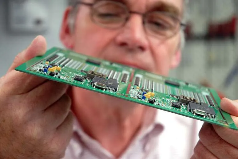
Tip: Use a profilometer to measure surface roughness after etching to ensure consistency. This small investment in quality control can prevent costly plating failures.
4. Improper Use of PCB Process Fluids
The choice and management of PCB process fluids play a huge role in pre-treatment success. Using expired or contaminated fluids for cleaning, degreasing, or etching can introduce impurities onto the board, directly contributing to plating failure. For instance, a contaminated etching solution might leave behind unwanted residues, reducing the effectiveness of the plating bath and causing defects like pitting or incomplete coverage.
A practical approach is to maintain a strict schedule for fluid replacement and filtration. Data from industry studies suggest that replacing process fluids after every 500 boards processed can reduce contamination-related defects by 40%. Additionally, store fluids in clean, sealed containers to prevent exposure to dust or moisture.
Tip: Implement a fluid analysis program to test for pH, concentration, and contaminant levels. This proactive step can extend fluid life while maintaining pre-treatment quality.
5. Skipping or Rushing Activation Steps
Activation, often involving a chemical treatment to prepare the surface for plating, is sometimes overlooked or rushed in the pre-treatment process. This step typically uses a palladium-based solution to create catalytic sites on the board for electroless plating. Skipping or inadequately performing activation can result in non-uniform plating or complete failure to deposit metal in certain areas.
For example, insufficient immersion time in the activation bath—sometimes as little as 30 seconds less than recommended—can reduce the density of catalytic sites by 50%, leading to spotty plating. Follow the precise timing and temperature guidelines for activation, often around 40-50°C for 2-5 minutes, depending on the solution used.
Tip: Use automated equipment to control immersion times and temperatures during activation for consistent results across batches.
6. Inconsistent Rinse Between Steps
Rinsing between pre-treatment steps is often underestimated, yet it’s vital to prevent cross-contamination. Failing to rinse thoroughly after cleaning, degreasing, or etching can carry over chemicals into the next process, disrupting the surface preparation. For instance, residual etching solution can react with the activation bath, reducing its effectiveness and causing uneven plating.
Always use high-purity deionized water for rinsing, and ensure multiple rinse cycles if necessary. A single rinse may not remove all traces of chemicals, especially in complex board designs with vias or tight spaces. Industry best practices suggest a minimum of two rinse cycles with water purity levels below 10 microsiemens/cm for optimal results.
Tip: Monitor rinse water conductivity to detect contamination early and maintain rinse tank cleanliness to avoid introducing new impurities.
Consequences of Plating Failure Due to Pre-Treatment Errors
The impact of poor pre-treatment can be severe, affecting both the functionality and reliability of the final PCB. Common consequences include:
- Poor Adhesion: Leads to peeling or flaking of the plated layer, causing open circuits or shorts.
- Uneven Plating: Results in inconsistent conductivity, affecting signal speeds by up to 10% in high-speed designs.
- Reduced Durability: Increases the risk of corrosion or mechanical failure under stress.
- High Rework Costs: Defects often require costly rework or scrapping of entire batches, impacting production timelines.
By addressing pre-treatment mistakes, manufacturers can significantly reduce defect rates and improve overall board quality.
Best Practices to Avoid Plating Failure
To ensure successful plating, follow these best practices during pre-treatment:
- Standardize Processes: Create detailed SOPs (Standard Operating Procedures) for each pre-treatment step to maintain consistency.
- Train Staff: Educate team members on the importance of each pre-treatment stage and proper handling of PCB process fluids.
- Invest in Quality Control: Use inspection tools like microscopes and surface testers to verify cleanliness and roughness after each step.
- Maintain Equipment: Regularly clean and calibrate tanks, pumps, and other equipment to prevent contamination or process deviations.
- Document Results: Keep records of fluid changes, process parameters, and defect rates to identify patterns and areas for improvement.
Conclusion
Pre-treatment is the foundation of successful plating in PCB manufacturing. Mistakes in plating pretreatment, such as inadequate cleaning PCBs, improper degreasing PCBs, errors in the etching process, or mismanagement of PCB process fluids, can lead to significant electroplating issues. By understanding these common errors and implementing the best practices outlined in this guide, you can minimize plating failures, reduce production costs, and deliver high-quality PCBs that meet stringent performance standards.
Attention to detail in every pre-treatment step—from cleaning to activation—ensures a robust foundation for plating. With consistent processes and quality control, you’ll achieve reliable adhesion, uniform metal deposition, and durable boards ready for any application.


