 ALLPCB


When designing a printed circuit board (PCB), one of the critical decisions you'll face is choosing the right type of via for your layout. Vias are essential for connecting different layers of a PCB, but not all vias are created equal. So, what's the difference between via-in-pad and traditional vias, and which one should you use? In short, via-in-pad is ideal for high-density designs with limited space, especially for fine-pitch components, while traditional vias, such as through-hole vias, are better suited for simpler, less compact boards where cost and ease of manufacturing are priorities. This blog will dive deep into the comparison of via-in-pad vs. through-hole via, via-in-pad vs. microvia, and via-in-pad vs. blind via, while also exploring when to use via-in-pad in your PCB design.
What Are Vias and Why Do They Matter in PCB Design?
Vias are small conductive pathways that allow electrical connections between different layers of a PCB. Without vias, multilayer boards wouldn't be able to function as signals and power couldn't travel between layers. The type of via you choose impacts your board's performance, manufacturability, and cost. Whether you're working on a high-speed digital circuit or a compact IoT device, understanding the strengths and limitations of each via type is crucial for a successful design.
In this post, we'll explore via-in-pad technology and compare it to traditional via types, helping you make an informed decision for your next project. Let's start by breaking down what via-in-pad and traditional vias are.
What is Via-in-Pad Technology?
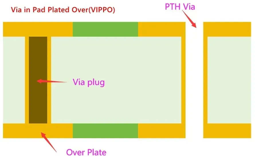
Via-in-pad (VIP) is a design technique where a via is placed directly under or within the pad of a surface-mount component. Unlike traditional vias that are placed outside the component pads, via-in-pad allows for a more compact layout by eliminating the need for additional routing space. To prevent solder from flowing into the via during assembly, these vias are typically filled with a conductive or non-conductive material and then plated over to create a flat, solderable surface.
This technology is particularly useful in high-density interconnect (HDI) designs where space is at a premium. By placing vias directly under components, you can reduce the board size and improve signal integrity by shortening trace lengths. However, via-in-pad often comes with higher manufacturing costs due to the additional processes involved in filling and plating the vias.
What Are Traditional Vias?
Traditional vias refer to the more conventional types of vias used in PCB design, including through-hole vias, blind vias, and buried vias. These vias are typically placed away from component pads, requiring additional space for routing traces. Here's a quick overview of the main types of traditional vias:
- Through-Hole Via: These vias go through the entire PCB, connecting the top and bottom layers as well as any internal layers in between. They are the most common and cost-effective type of via but take up more space.
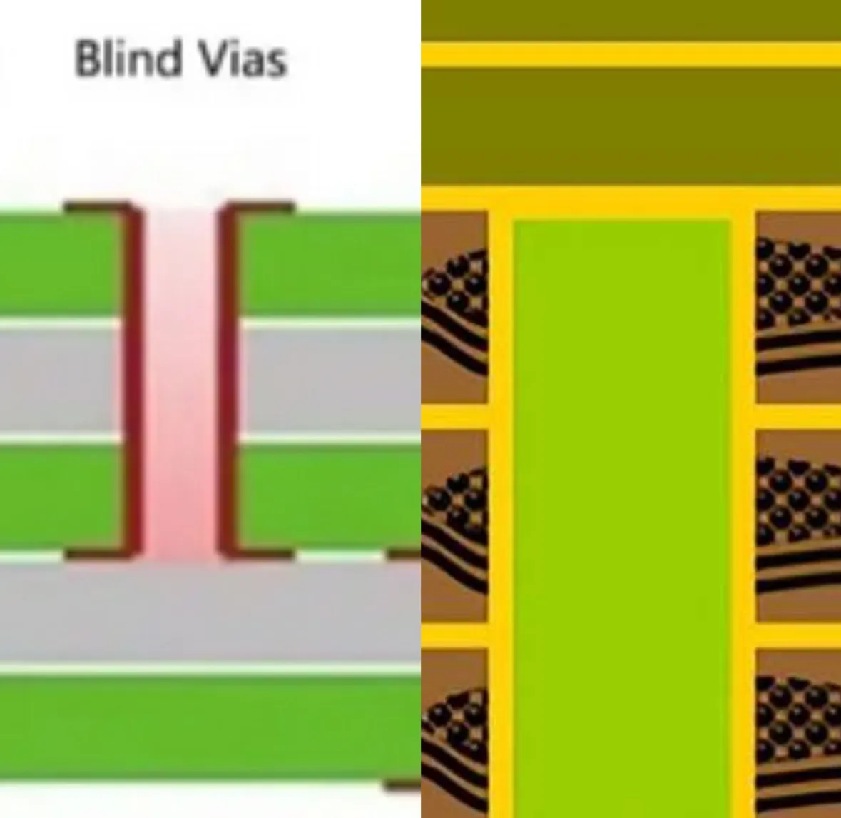
- Blind Via: These vias connect an outer layer to an inner layer but do not go through the entire board. They save space compared to through-hole vias but are more expensive to manufacture.
- Buried Via: These vias connect only internal layers and are not visible on the outer surfaces of the PCB. They are ideal for HDI designs but add complexity and cost to manufacturing.
Traditional vias are widely used in designs where space constraints are not a major concern, and cost-effective production is a priority.
Via-in-Pad vs. Through-Hole Via: Key Differences
When comparing via-in-pad vs. through-hole via, the primary difference lies in placement and application. Through-hole vias are drilled through the entire PCB and are placed outside component pads, often requiring additional traces to connect to the pads. This can increase the overall size of the board and potentially introduce signal integrity issues due to longer trace lengths.
In contrast, via-in-pad places the via directly under the component pad, saving space and reducing trace length. For example, in a design with a fine-pitch BGA (Ball Grid Array) component with a 0.5mm pitch, using via-in-pad can eliminate the need for dog-bone routing (a small trace connecting the pad to a nearby via), which would otherwise clutter the layout. However, through-hole vias are simpler and cheaper to manufacture since they don't require filling or plating processes. A typical through-hole via might have a diameter of 0.3mm to 0.5mm, while via-in-pad designs often use smaller diameters (around 0.2mm) to fit within the pad area.
In terms of performance, via-in-pad can reduce parasitic inductance and improve signal integrity, especially in high-speed designs where signal delays must be minimized. For instance, a shorter connection path can reduce signal propagation delay by a few picoseconds, which is critical in applications like DDR memory interfaces operating at speeds above 1 GHz.
Via-in-Pad vs. Microvia: Understanding the Distinction
Now, let's look at via-in-pad vs. microvia. A microvia is a small via, typically with a diameter of less than 0.15mm, often drilled using a laser. Microvias are commonly used in HDI designs to connect adjacent layers, and they can be blind (connecting an outer layer to an inner layer) or buried (connecting internal layers only). While via-in-pad can use microvias, not all microvias are placed in pads.
The key difference is that via-in-pad refers to the placement of the via under a component pad, while microvia refers to the size and manufacturing method of the via. For example, a microvia with a diameter of 0.1mm and an aspect ratio (depth-to-diameter) of 1:1 might be used in a via-in-pad design to connect a surface layer to an inner layer under a 0.4mm pitch component. However, microvias can also be placed outside pads in tight routing areas, making them versatile for HDI PCBs.
Both via-in-pad and microvias are suited for compact designs, but via-in-pad often involves additional steps like filling and plating, which can increase costs compared to standard microvias. If your design doesn't require vias directly under pads, using microvias outside pads can still achieve a high-density layout at a lower cost.
Via-in-Pad vs. Blind Via: Placement and Purpose
Comparing via-in-pad vs. blind via, the distinction again lies in placement and purpose. A blind via connects an outer layer to an inner layer without passing through the entire board. Like microvias, blind vias are often used in HDI designs to save space and reduce layer count. However, blind vias are typically placed outside component pads unless they are part of a via-in-pad design.
In a via-in-pad setup, a blind via might be used to connect the surface pad to a power or ground plane on an inner layer, reducing the via's footprint on the bottom side of the board. For instance, in a 6-layer PCB, a blind via might span only from layer 1 to layer 2, with a depth of 0.2mm, allowing for more routing space on the lower layers. On the other hand, a standard blind via placed outside a pad might serve the same purpose but require additional trace length, potentially increasing signal loss or crosstalk in high-frequency designs (e.g., above 5 GHz).
Blind vias are generally more expensive than through-hole vias but less costly than via-in-pad if no filling or plating is required. Choosing between these depends on whether your design prioritizes space under components or overall layer efficiency.
When to Use Via-in-Pad in PCB Design
Knowing when to use via-in-pad is crucial for optimizing your PCB design. Here are the key scenarios where via-in-pad technology shines:
- High-Density Designs: If you're working on a board with fine-pitch components, such as BGAs or QFNs with pitches below 0.8mm, via-in-pad allows you to place vias directly under the pads, saving valuable board space and simplifying routing.
- Limited Surface Routing Options: When surface layers are congested with components and traces, via-in-pad helps by moving connections directly beneath pads, reducing the need for complex routing patterns.
- Improved Signal Integrity: In high-speed designs, shorter trace lengths are critical. Via-in-pad minimizes trace length, reducing parasitic effects like inductance and capacitance. For example, in a design operating at 10 Gbps, minimizing inductance to below 1 nH can be achieved more easily with via-in-pad.
- Thermal Management: Via-in-pad can also aid in heat dissipation by connecting thermal pads directly to inner copper planes. A filled via with conductive material can transfer heat more efficiently, maintaining component temperatures within safe limits (e.g., below 85°C for most ICs).
However, via-in-pad is not always the best choice. If your design has ample space and doesn't involve fine-pitch components or high-speed signals, traditional vias like through-hole or blind vias might be more cost-effective. The added manufacturing steps for via-in-pad, such as resin filling and copper plating, can increase production costs by 20-30% compared to standard via processes.
Pros and Cons of Via-in-Pad Technology
To help you weigh your options, here's a breakdown of the advantages and disadvantages of via-in-pad:
Advantages:
- Saves space on the PCB, enabling smaller, more compact designs.
- Reduces trace length, improving signal integrity for high-speed applications.
- Supports fine-pitch components by eliminating the need for external routing.
- Enhances thermal dissipation when used with conductive fill materials.
Disadvantages:
- Higher manufacturing costs due to additional processes like filling and plating.
- Increased risk of assembly issues if vias are not properly filled, leading to solder voids or poor connections.
- More complex design rules, requiring careful planning to avoid manufacturing defects.
Pros and Cons of Traditional Vias
For comparison, here's a look at the strengths and weaknesses of traditional vias:
Advantages:
- Lower manufacturing costs, especially for through-hole vias.
- Simpler design and fabrication process, reducing the risk of errors.
- Suitable for a wide range of applications, from simple to moderately complex designs.
Disadvantages:
- Takes up more space, which can be a problem in high-density designs.
- Longer trace lengths can degrade signal integrity in high-speed circuits.
- Limited flexibility for fine-pitch components without additional routing complexity.
Design Tips for Using Via-in-Pad
If you decide to use via-in-pad in your PCB design, keep these practical tips in mind to ensure success:
- Work with Your Manufacturer Early: Not all PCB fabricators support via-in-pad technology due to the specialized processes involved. Discuss your design requirements with your manufacturer to confirm capabilities and avoid costly redesigns.
- Choose the Right Fill Material: Decide whether to use conductive or non-conductive fill based on your thermal and electrical needs. Conductive fills improve heat transfer but may introduce unwanted capacitance in high-frequency designs.
- Optimize Via Size: Use smaller via diameters (e.g., 0.2mm or less) to fit within component pads, but ensure they meet the aspect ratio requirements for reliable drilling and plating (typically 1:1 for microvias).
- Plan for Assembly: Ensure that vias are properly capped or plated to create a flat surface for soldering. Poorly filled vias can lead to solder wicking, causing weak joints or open circuits.
Conclusion: Making the Right Choice for Your PCB
Choosing between via-in-pad and traditional vias comes down to the specific needs of your PCB design. If you're dealing with high-density layouts, fine-pitch components, or high-speed signals, via-in-pad offers significant advantages in space savings and performance. However, for simpler designs where cost and ease of manufacturing are more important, traditional vias like through-hole or blind vias are often the better choice.
By understanding the differences between via-in-pad vs. through-hole via, via-in-pad vs. microvia, and via-in-pad vs. blind via, as well as knowing when to use via-in-pad, you can make an informed decision that balances performance, cost, and manufacturability. Whether you're designing a compact wearable device or a robust industrial controller, selecting the right via type is a key step in ensuring your PCB meets its performance goals.


