 ALLPCB


If you're designing high-speed printed circuit boards (PCBs), mastering plated through-hole (PTH) design is critical for ensuring signal integrity and performance. PTH vias connect different layers of a PCB, but in high-speed applications, they can introduce challenges like impedance mismatches and signal delays if not designed properly. In this comprehensive guide, we'll dive deep into PTH design rules, high-speed PCB vias, impedance control for PTH, signal integrity with plated through-holes, and differential pair routing with PTH. Whether you're a seasoned engineer or new to PCB design, this guide offers practical tips and detailed insights to help you optimize your high-speed PCB layouts.
What Are Plated Through-Holes (PTH) and Why Do They Matter in High-Speed PCBs?
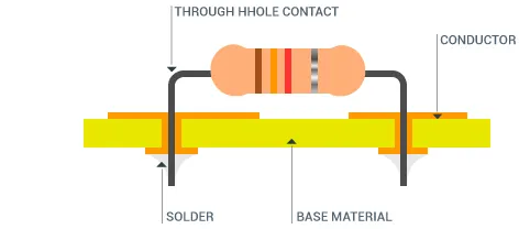
Plated through-holes are small, conductive holes drilled through a PCB to create electrical connections between layers. Unlike non-plated holes, PTHs have a thin layer of copper plated inside, ensuring reliable conductivity. In high-speed PCBs, where signals travel at frequencies often exceeding 1 GHz, PTH vias play a pivotal role in maintaining signal quality. Poorly designed PTHs can cause reflections, crosstalk, and signal loss, leading to system failures.
In high-speed designs, every element, including vias, impacts performance. PTH vias must be carefully planned to minimize disruptions to signal paths. Let’s explore how to design them effectively by focusing on key aspects like impedance control, signal integrity, and routing strategies.
Key PTH Design Rules for High-Speed PCBs
Designing PTH vias for high-speed PCBs requires adherence to specific rules to avoid performance issues. Below are the most important guidelines to follow:
1. Minimize Via Stub Lengths
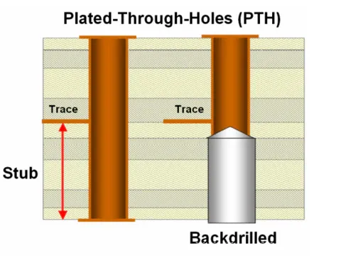
In high-speed designs, via stubs (the unused portion of a via after the signal transitions to another layer) act as antennas, causing signal reflections. For signals operating at 5 GHz, a stub longer than 0.5 mm can introduce significant noise. Use back-drilling to remove unused stub sections or opt for blind and buried vias if your design allows.
2. Optimize Via Diameter and Pad Size
Smaller via diameters reduce parasitic capacitance and inductance, which are critical for maintaining signal integrity at high frequencies. A typical via diameter for high-speed designs ranges from 0.2 mm to 0.3 mm, with pad sizes around 0.5 mm to 0.6 mm. Ensure that the via size supports the current-carrying capacity while minimizing signal distortion.
3. Place Vias Strategically
Avoid placing PTH vias directly in the path of high-speed signals unless necessary. If a via is required, position it to minimize trace length disruptions. For instance, placing vias at the end of a trace rather than in the middle can reduce signal path interruptions.
Impedance Control for PTH in High-Speed Designs
Impedance control is a cornerstone of high-speed PCB design, and PTH vias can disrupt the characteristic impedance of a signal path if not managed properly. Here’s how to ensure impedance control with PTH:
1. Match Via Impedance to Trace Impedance
High-speed signals often require a controlled impedance, such as 50 ohms for single-ended traces or 100 ohms for differential pairs. A PTH via introduces inductance and capacitance, altering the impedance. To counteract this, adjust the via pad size and anti-pad (the clearance area around the via in the ground plane). For a 50-ohm trace, an anti-pad diameter of 0.8 mm to 1.0 mm often works well, though simulation tools can provide precise values for your stack-up.
2. Use Ground Vias for Return Paths
Place ground vias near high-speed signal vias to provide a low-impedance return path. This reduces loop inductance and minimizes electromagnetic interference (EMI). A common practice is to place one ground via for every signal via within a 1 mm radius.
3. Simulate Via Effects
Use electromagnetic simulation software to model the impedance of PTH vias in your design. Tools can predict how vias affect signal behavior at frequencies above 1 GHz, allowing you to tweak parameters like via spacing and pad size before fabrication.
Ensuring Signal Integrity with Plated Through-Holes
Signal integrity refers to the preservation of a signal’s quality as it travels through a PCB. PTH vias can degrade signal integrity if not designed with care. Here are strategies to maintain signal integrity in high-speed designs:
1. Reduce Crosstalk with Proper Spacing
Crosstalk occurs when signals in adjacent vias interfere with each other. To prevent this, maintain a minimum spacing of at least three times the via diameter between high-speed signal vias. For example, with a 0.3 mm via diameter, keep a spacing of 0.9 mm or more.
2. Avoid Via Transitions in Critical Nets
Each time a signal transitions through a via to another layer, it encounters impedance discontinuities. Limit the number of via transitions for critical high-speed nets. If transitions are unavoidable, ensure that the via is surrounded by a solid ground plane to minimize noise.
3. Use High-Quality Materials
The dielectric material of your PCB affects how signals behave around PTH vias. Low-loss materials with a dielectric constant (Dk) of 3.0 to 3.5 are ideal for frequencies above 10 GHz, as they reduce signal attenuation near vias.
Differential Pair Routing with PTH in High-Speed PCBs
Differential pairs are commonly used in high-speed designs for protocols like USB, PCIe, and Ethernet, where two signals carry complementary data to reduce noise. Routing differential pairs through PTH vias requires precision to maintain signal balance and timing. Here’s how to do it right:
1. Keep Differential Vias Symmetrical
Place the vias for a differential pair as close together as possible while maintaining symmetry. Uneven spacing can cause skew, where one signal arrives before the other, disrupting timing. A spacing of 0.5 mm to 0.8 mm between differential vias often works well for signals up to 5 GHz.
2. Match Trace Lengths Before and After Vias
Length mismatches in differential pairs lead to phase differences, degrading performance. Ensure that the trace lengths on both sides of the vias are equal. If one trace must be longer due to via placement, use serpentine routing to match the lengths within 0.1 mm.
3. Surround Differential Vias with Ground Planes
To shield differential pairs from external noise, place ground vias around the pair. This creates a controlled environment, reducing EMI and crosstalk. A ring of four to six ground vias around the differential pair vias is a common practice for signals above 3 GHz.
Advanced Tips for High-Speed PCB Vias and PTH Design
Beyond the basics, here are some advanced strategies to further optimize PTH design in high-speed PCBs:
1. Use Blind and Buried Vias
Blind vias (connecting an outer layer to an inner layer) and buried vias (connecting inner layers only) eliminate stubs, improving signal integrity. While these vias increase fabrication costs, they are worth considering for designs operating above 10 GHz.
2. Implement Via Stitching for Ground Planes
Via stitching involves placing multiple ground vias around high-speed signal paths to create a robust return path. This technique is especially useful in multilayer boards, where signals may traverse several layers through PTH vias. Space stitching vias at intervals of λ/10 (where λ is the wavelength of the highest signal frequency) to suppress resonances.
3. Test and Validate Designs
After designing your PCB, use time-domain reflectometry (TDR) to measure impedance discontinuities caused by PTH vias. This testing helps identify issues like reflections or mismatches before full production, saving time and cost.
Common Mistakes to Avoid in PTH Design for High-Speed PCBs
Even experienced designers can make errors when working with PTH vias in high-speed applications. Here are some pitfalls to watch out for:
- Ignoring Via Stubs: Failing to address stubs can lead to severe signal reflections, especially at frequencies above 1 GHz.
- Overcrowding Vias: Placing too many vias close together increases crosstalk and complicates routing.
- Neglecting Ground Planes: Without a solid ground plane near vias, return paths become longer, increasing inductance and EMI.
- Skipping Simulations: Not simulating via effects can result in unexpected performance issues that are costly to fix after fabrication.
Conclusion: Mastering PTH Design for High-Speed PCB Success
Plated through-hole design is a critical aspect of high-speed PCB development. By following PTH design rules, focusing on impedance control, ensuring signal integrity, and optimizing differential pair routing, you can create boards that perform reliably even at the highest frequencies. Remember to minimize via stubs, use ground vias for return paths, and simulate your designs to catch issues early. With these strategies, you'll be well-equipped to tackle the challenges of high-speed PCB design and deliver top-notch results.


