 ALLPCB


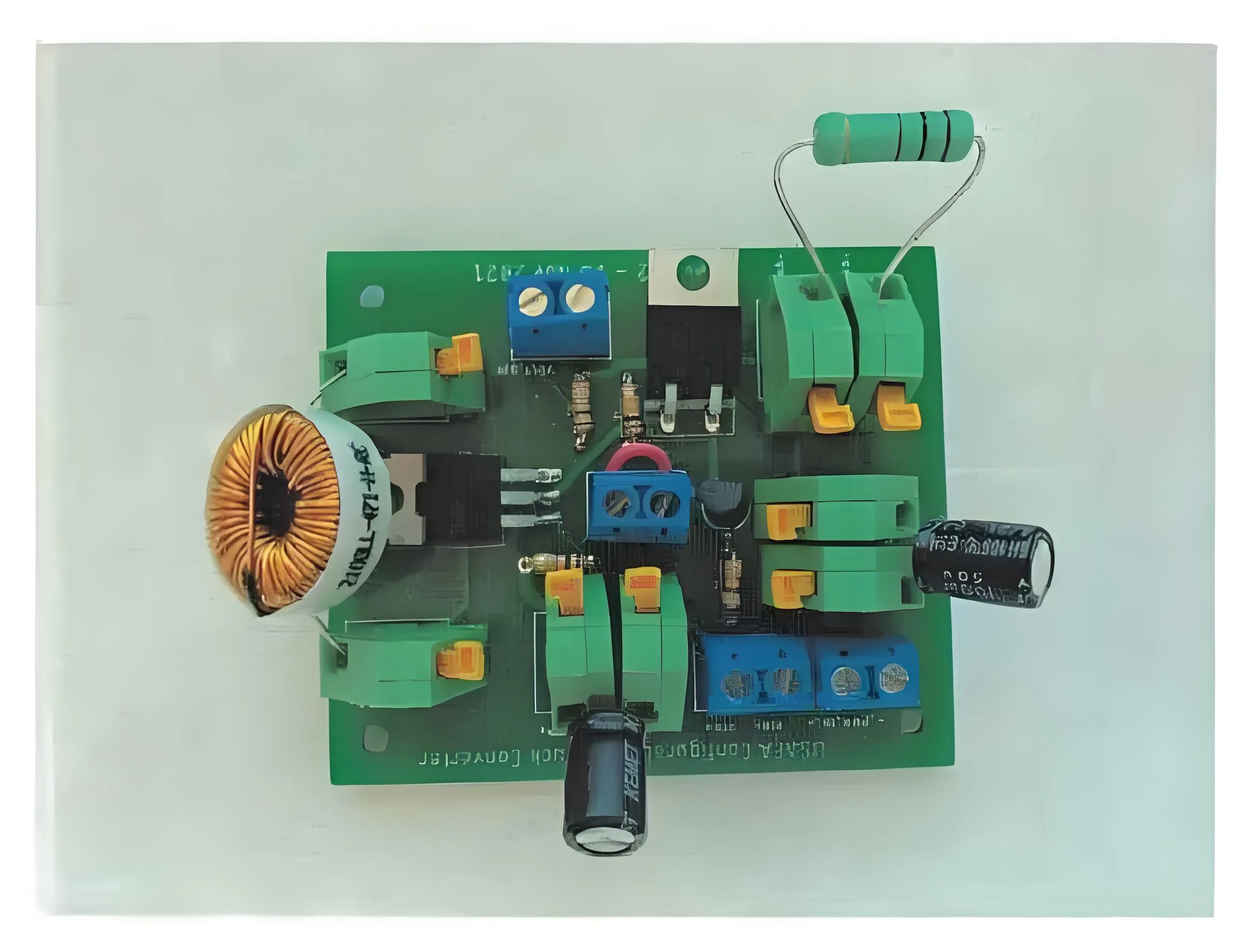
In the world of electronics design, creating an efficient switch PCB layout is critical for ensuring optimal performance. A well-designed PCB for switches, such as those used in power supplies or high-frequency circuits, can significantly reduce electromagnetic interference (EMI) and noise. This blog post dives deep into switch PCB layout guidelines, offering actionable tips on EMI reduction in PCB, noise minimization techniques, PCB grounding strategies, and power plane design. Whether you're an experienced engineer or just starting, these best practices will help you design robust and reliable circuits.
Why Switch PCB Layout Matters for EMI and Noise Control
Switching circuits, especially in power electronics, are notorious for generating EMI and noise due to rapid changes in current and voltage. These disturbances can interfere with nearby components or even other devices, leading to performance issues or failure to meet regulatory standards. A carefully planned switch PCB layout minimizes these problems by controlling signal paths, reducing loop areas, and optimizing grounding. In the sections below, we'll explore proven strategies to achieve this.
Key Principles of Switch PCB Layout Guidelines
Designing a switch PCB layout requires attention to detail and adherence to fundamental principles. Here are the core guidelines to follow for reducing EMI and noise:
1. Minimize Loop Areas in High-Current Paths
In switching circuits, high-frequency currents flow through specific paths, often creating loops that act as antennas for EMI radiation. To reduce this, keep the loop area as small as possible. For instance, in a buck converter circuit, place the input capacitor close to the switching MOSFET and the diode to shorten the current loop. A smaller loop area can reduce radiated EMI by up to 20-30% in some designs, depending on frequency and current levels.
2. Optimize Component Placement
Place critical components like switching elements, inductors, and capacitors strategically. Keep high-frequency components close together to reduce trace lengths, which lowers inductance and the chance of noise pickup. For example, in a switch-mode power supply, position the control IC near the switching transistor to avoid long, noisy control lines. This can cut down signal delays and reduce noise coupling by maintaining trace lengths under 10-15 mm for high-speed signals.
3. Use Short and Wide Traces for Power Paths
Long, thin traces in power paths increase resistance and inductance, leading to voltage drops and noise. Use short, wide traces for high-current paths to handle currents efficiently. A trace width of 20-30 mils per ampere of current is a common rule of thumb for power traces on a 1 oz copper PCB. This minimizes resistive losses and helps with heat dissipation, reducing noise in the system.
EMI Reduction in PCB: Practical Techniques
Electromagnetic interference is a major challenge in switch PCB designs, especially at frequencies above 100 kHz. Here are specific techniques to achieve EMI reduction in PCB layouts:
1. Implement EMI Filters
Add EMI filters at the input and output of your switching circuit to suppress high-frequency noise. A common approach is to use a pi-filter (capacitor-inductor-capacitor) at the input to block conducted EMI. For instance, a filter with a 10 μH inductor and 1 μF capacitors can attenuate noise above 1 MHz effectively in many designs. Ensure the filter components are placed close to the power entry point for maximum impact.
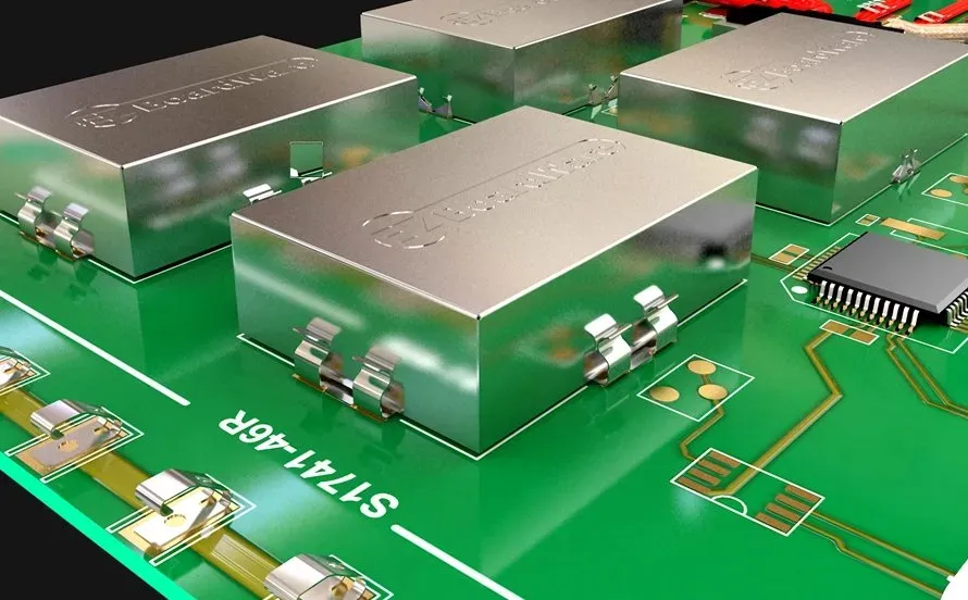
2. Shield Sensitive Areas
For high-frequency switching circuits, consider using shielding techniques. Place a ground plane or copper pour around sensitive analog components to block radiated EMI. If possible, use metal enclosures or cans over critical sections of the PCB. This can reduce EMI pickup by up to 40 dB in some cases, depending on the frequency and shielding material.
3. Control Switching Frequency and Slew Rate
The switching frequency and slew rate directly affect EMI generation. Slower slew rates reduce high-frequency harmonics, thus lowering EMI. If your design allows, use a switching frequency below 500 kHz to stay within safer EMI limits for many applications. Additionally, add gate resistors (e.g., 10-100 ohms) to slow down MOSFET switching transitions, balancing efficiency and EMI reduction.
Noise Minimization Techniques for Switch PCBs
Noise in switching circuits can degrade signal integrity and affect overall performance. Here are effective noise minimization techniques to incorporate into your design:
1. Separate Analog and Digital Sections
Mixing analog and digital signals on the same plane can lead to crosstalk and noise coupling. Physically separate analog and digital components on the PCB, and route their traces away from each other. For mixed-signal designs, use a split ground plane with a single connection point to avoid ground loops, which can introduce noise at levels as low as a few millivolts but still disrupt sensitive circuits.
2. Use Decoupling Capacitors Effectively
Place decoupling capacitors close to the power pins of ICs to filter out high-frequency noise. A 0.1 μF ceramic capacitor paired with a 10 μF electrolytic capacitor can cover a wide range of frequencies, stabilizing the power supply. Ensure the capacitor leads are short (less than 5 mm) to minimize parasitic inductance, which can otherwise negate the filtering effect.
3. Route Signals Away from Noise Sources
Keep sensitive signal traces away from high-current switching paths and inductors, which are major noise sources. Use perpendicular routing for signal and power traces to minimize coupling. If traces must cross, ensure they do so at a 90-degree angle to reduce capacitive noise coupling by up to 50% compared to parallel routing over long distances.
PCB Grounding Strategies for Optimal Performance
Grounding is one of the most critical aspects of switch PCB design. Poor grounding can lead to noise, EMI, and signal integrity issues. Here are essential PCB grounding strategies to follow:
1. Use a Solid Ground Plane
A continuous ground plane on one layer of the PCB provides a low-impedance path for return currents, reducing noise and EMI. Avoid splitting the ground plane under high-frequency traces, as this forces return currents to take longer paths, increasing loop areas and EMI. For a 4-layer PCB, dedicate one layer entirely to ground to achieve impedance values as low as 0.1 ohms or less for return paths.
2. Implement Star Grounding for Mixed Signals
In designs with both analog and digital sections, use a star grounding approach. Connect all ground points to a single node to prevent ground loops. This technique ensures that noisy digital currents don’t interfere with sensitive analog signals, maintaining signal integrity even at low voltage levels like 1-2 mV.
3. Place Ground Vias Strategically
In multi-layer PCBs, use multiple ground vias to connect components to the ground plane. Place vias close to component ground pins (within 3-5 mm) to minimize return path inductance. For high-current designs, use at least 2-3 vias per ground connection to handle currents up to 5A without significant voltage drops.
Power Plane Design: Best Practices for Stability
A well-designed power plane ensures stable voltage delivery and minimizes noise in switching circuits. Follow these power plane design best practices:
1. Dedicate a Layer for Power Distribution
In multi-layer PCBs, dedicate an entire layer to the power plane to provide a low-impedance path for current distribution. This reduces voltage drops and noise, especially in high-current switching applications. For a 5V rail carrying 3A, a solid power plane can keep voltage ripple below 50 mV under load.
2. Use Wide Power Traces or Polygons
For single or double-layer boards where a full power plane isn't feasible, use wide traces or copper polygons for power distribution. A width of 50-100 mils for a 2A current path ensures minimal resistance (around 1-2 milliohms per inch) and reduces heat buildup, contributing to noise reduction.
3. Place Power and Ground Planes Adjacent
In multi-layer designs, place power and ground planes on adjacent layers to create a natural capacitance between them. This capacitance, often around 1-2 nF per square inch for standard FR4 material with 8 mil separation, helps filter high-frequency noise and stabilize the power supply.
Additional Tips for Switch PCB Layout Success
Beyond the core strategies, consider these additional tips to enhance your switch PCB layout:
- Thermal Management: Switching components like MOSFETs generate heat. Use thermal vias and copper pours to dissipate heat, preventing noise from thermal stress. Aim for a thermal resistance below 10°C/W for high-power components.
- Simulation Tools: Use PCB design software with simulation capabilities to analyze EMI and noise before manufacturing. Tools can predict loop inductance and suggest layout improvements, saving time and cost.
- Compliance with Standards: Ensure your design meets EMI standards like FCC Part 15 or CISPR 22 for conducted and radiated emissions. Test early with a spectrum analyzer to identify problem frequencies, often in the 30-300 MHz range for switching circuits.
Conclusion: Building Better Switch PCB Layouts
Designing a switch PCB layout that minimizes EMI and noise is a blend of science and art. By following the switch PCB layout guidelines outlined here, such as minimizing loop areas, optimizing grounding, and using solid power planes, you can significantly improve your circuit's performance. Techniques for EMI reduction in PCB and noise minimization ensure compliance with standards and reliable operation. Strong PCB grounding strategies and power plane design further enhance stability and signal integrity.
At ALLPCB, we're committed to supporting engineers with resources and manufacturing solutions to bring their designs to life. Apply these best practices in your next project to create efficient, low-noise switching circuits that stand the test of time.


