 ALLPCB


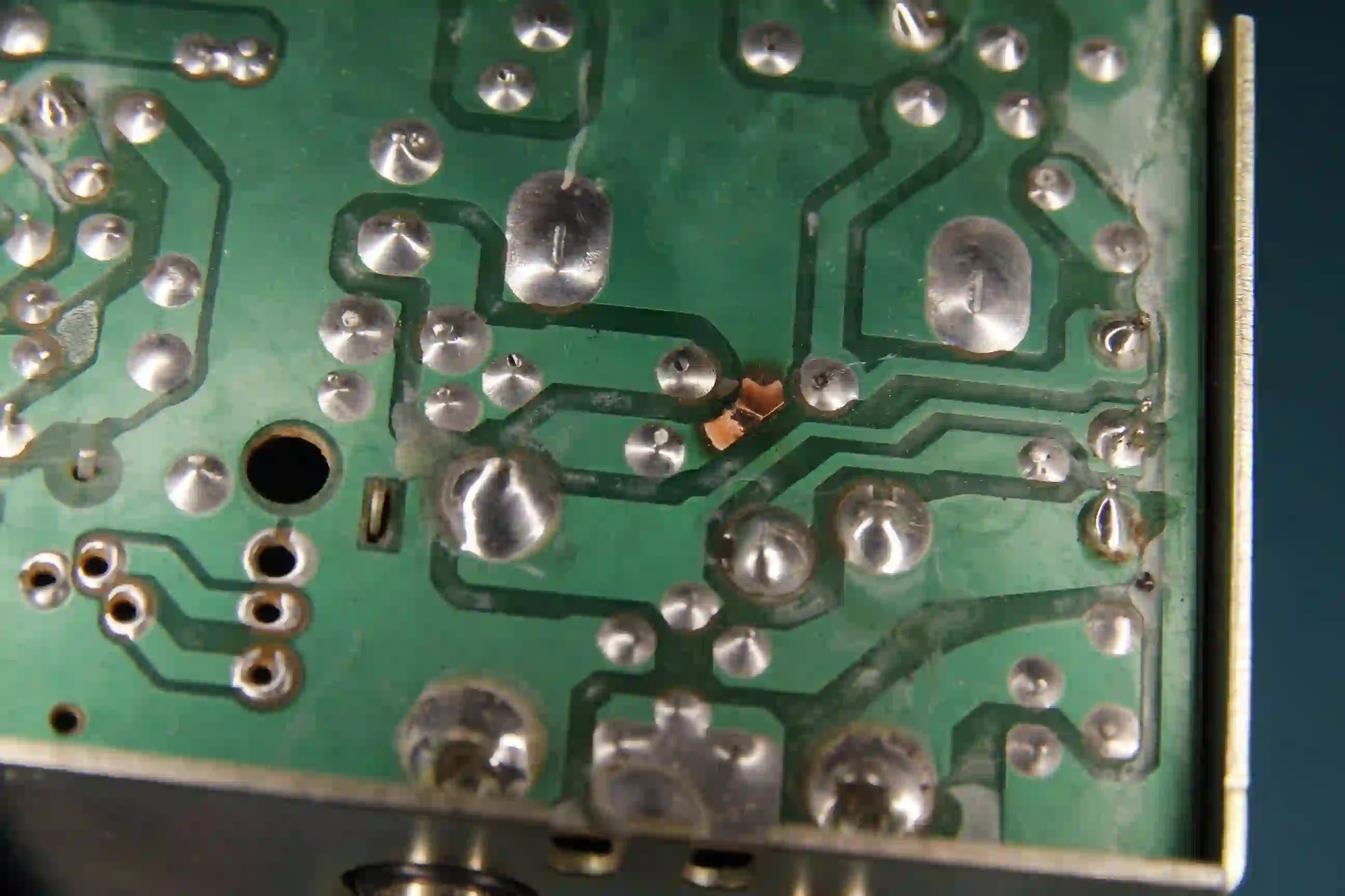
Printed circuit boards (PCBs) are the backbone of modern electronics, enabling devices from smartphones to industrial machinery to function seamlessly. However, damaged PCB traces—those thin copper pathways that connect components—can disrupt electrical flow, leading to malfunctions or complete device failure. Whether caused by physical stress, corrosion, or overheating, trace damage doesn't always mean a board is beyond saving. With the right tools and techniques, engineers can repair these critical pathways and restore functionality.
In this step-by-step tutorial, we'll guide you through the process of repairing damaged PCB traces, offering practical advice and expert tips to ensure reliable repairs. From identifying breaks to soldering jumper wires, we'll cover everything you need to know to bring your PCB back to life.
Understanding PCB Trace Damage
PCB traces are delicate copper pathways, typically 0.1 mm to 0.5 mm wide, that conduct electrical signals between components. Damage to these traces can occur due to several reasons:
- Physical Stress: Dropping a device or mishandling during assembly can crack or break traces. For example, excessive force when inserting a plug-in board may fracture a 0.2 mm trace.
- Corrosion: Exposure to moisture or chemicals, such as a leaky electrolytic capacitor, can erode copper traces, increasing resistance and disrupting signal integrity.
- Overheating: Prolonged exposure to high temperatures during soldering (e.g., above 260°C for more than 10 seconds) can lift or burn traces, especially on FR4 substrates.
- Poor Design: Inadequate trace width for high-current applications (e.g., a 0.3 mm trace carrying 2 A) can lead to overheating and failure.
Understanding the cause of damage helps determine the best repair approach. For instance, corrosion may require extensive cleaning, while a clean break might only need a jumper wire.
Tools and Materials Needed
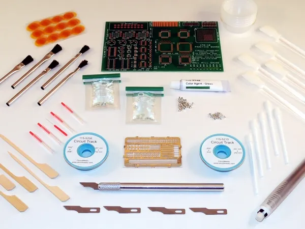
Before starting the repair, gather the following tools and materials to ensure precision and safety:
- Soldering Iron (15-30 W): A temperature-controlled soldering station is ideal for delicate work. Use a fine tip (e.g., 1 mm) for precision.
- Solder and Flux: Use rosin-core solder (0.5-1 mm diameter) and liquid flux to ensure clean joints.
- Multimeter: Essential for testing continuity (e.g., resistance < 1 Ω indicates a good connection).
- Conductive Ink Pen: For small trace repairs, silver-based pens offer low resistance (0.2-3 Ω over 1 mm).
- Jumper Wires: 30 AWG wire-wrap wire is ideal for bridging larger breaks.
- Copper Tape: Adhesive-backed tape (0.1-0.5 mm thick) for replacing lifted traces.
- Precision Tweezers: For handling small wires and components.
- Isopropyl Alcohol (99%): For cleaning corrosion and flux residue.
- Magnifying Glass or Microscope: To inspect traces as small as 0.1 mm.
- UV Solder Mask and Conformal Coating: To protect repaired areas from environmental damage.
Having these tools on hand streamlines the repair process and minimizes the risk of further damage.
Step-by-Step Guide to Repairing PCB Traces
Step 1: Diagnose the Damage
Start by visually inspecting the PCB under good lighting. Use a magnifying glass or microscope to spot cracks, burns, or corrosion. For example, a corroded trace may appear dull or greenish, while a burned trace might be blackened.
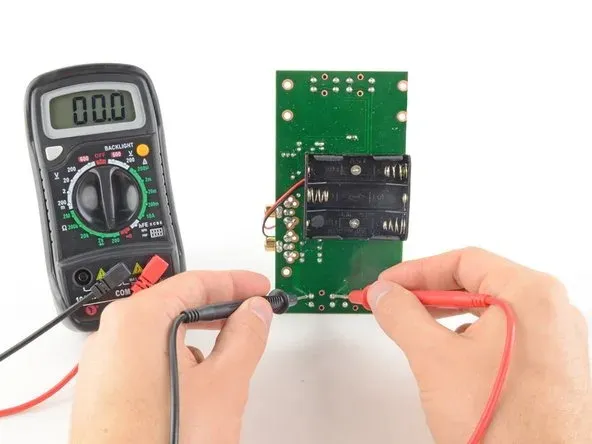
Next, use a multimeter in continuity mode to confirm the break. Place probes on either side of the suspected trace; no beep or infinite resistance indicates an open circuit. For instance, a healthy 10 mm trace should have a resistance of less than 0.5 Ω.
Step 2: Clean the Damaged Area
Clean the area around the damaged trace to remove corrosion, solder mask, or debris. Use a fine blade or fiberglass pencil to scrape away the green solder mask until shiny copper is exposed (about 3 mm on either side of the break). Then, apply isopropyl alcohol with a Q-tip to remove residue.
For corrosion, neutralize any acid (e.g., from battery leaks) with a baking soda solution before cleaning. This prevents further degradation of the copper.
Step 3: Choose a Repair Method
Depending on the extent of the damage, select one of these repair methods:
- Conductive Ink for Small Breaks: For cracks less than 1 mm, apply silver-based conductive ink with a fine-tip pen. Ensure the ink overlaps the copper by 2 mm on each side. Allow it to dry for 5-10 minutes, or use gentle heat (e.g., 60°C) to speed up curing. Silver ink can handle currents up to 3 A for a 1 mm wide trace.
- Jumper Wire for Larger Breaks: For breaks wider than 1 mm or lifted traces, use a 30 AWG wire. Strip 2 mm of insulation from each end, tin the wire with solder, and solder it across the break, connecting to exposed copper or nearby solder joints.
- Copper Tape for Severe Damage: If a trace is completely missing, cut adhesive copper tape to match the original trace width (e.g., 0.3 mm). Apply it over the damaged area, solder the ends to the existing trace, and secure with epoxy for stability.
Step 4: Solder and Secure the Repair
For jumper wires or copper tape, apply flux to the exposed copper and solder the repair in place. Use minimal heat (e.g., 250°C for 2-3 seconds) to avoid lifting adjacent traces. Secure jumper wires with Kapton tape or epoxy to prevent movement.
Step 5: Test the Repair
Use a multimeter to verify continuity across the repaired trace. A resistance reading below 1 Ω indicates a successful repair. Power on the PCB and test its functionality, monitoring for issues like signal distortion or overheating.
For high-frequency signals (e.g., 100 MHz), ensure the repair maintains impedance. A poorly repaired trace may increase impedance by 10-20 Ω, causing signal degradation.
Suggested Reading:How PCB Trace Width Affects Impedance: A Practical Guide
Step 6: Protect the Repaired Area
Apply a UV-curable solder mask over the repaired trace to insulate it and protect against moisture and dust. Cure the mask under UV light for 10-20 seconds. Optionally, apply a conformal coating for additional environmental protection, especially for boards used in humid or dusty environments.
Tips for Successful PCB Trace Repairs
To maximize the reliability of your repairs, keep these tips in mind:
- Work in a Static-Free Environment: Use an anti-static wrist strap to prevent electrostatic discharge, which can damage sensitive components.
- Practice on Scrap Boards: If you're new to soldering or trace repair, practice on a non-critical board to hone your skills.
- Match Trace Widths: Ensure repair materials (e.g., copper tape or wire) match the original trace width to maintain current-carrying capacity and impedance.
- Double-Check Connections: After reflow soldering, inspect joints under magnification to ensure there are no cold solder joints or unintended bridges.
- Document Repairs: Note the location and method of each repair for future reference, especially for complex boards with multiple fixes.
Suggested Reading:The Ultimate PCB Trace Width Calculator Guide: Ensuring Safe Current Flow
How ALLPCB Supports Your PCB Needs
At ALLPCB, we understand the challenges engineers face when repairing or prototyping PCBs. Our quick-turn PCB manufacturing and assembly services ensure you have high-quality boards to work with, minimizing the risk of trace damage during PCB assembly.
Conclusion
Repairing damaged PCB traces is a valuable skill that can save time, money, and resources. By following this step-by-step guide, engineers can diagnose trace damage, select the appropriate repair method, and restore functionality with confidence. From conductive ink for small cracks to jumper wires for larger breaks, each technique offers a reliable solution when executed with care.
With the right tools, techniques, and support from partners like ALLPCB, you can tackle PCB trace repairs effectively and keep your electronics running smoothly. Start practicing these methods today, and turn damaged boards into fully functional circuits.





