ALLPCB


What Is PCB Aspect Ratio and Why It Matters
PCB aspect ratio refers to the relationship between the finished board thickness and the diameter of a drilled hole, expressed as a simple ratio. For example, a 2.0 mm thick board with a 0.25 mm diameter hole yields an aspect ratio of 8:1. In high-layer-count constructions, typical thicknesses range from 1.6 mm upward, pushing aspect ratios higher when small via diameters are required for dense interconnects.
This parameter directly affects manufacturability in high-layer-count PCB manufacturing. Higher ratios increase the difficulty of achieving uniform copper plating inside the hole walls and complicate mechanical drilling processes. Poor aspect ratio control can lead to voids, thin plating, or incomplete hole cleaning, compromising electrical performance and long-term reliability. Industry specifications such as IPC-6012E establish performance requirements that implicitly guide acceptable aspect ratios for rigid boards.
Technical Principles of Aspect Ratio in Drilling
Mechanical drilling remains the dominant method for creating through holes and vias in multilayer boards. As the drill bit penetrates thicker material stacks, chip evacuation becomes more challenging. Debris can accumulate along the hole walls, generating excess heat that may cause drill wander or smear resin. These effects intensify with rising aspect ratios because the flute length exposed to the workpiece grows relative to the hole diameter.
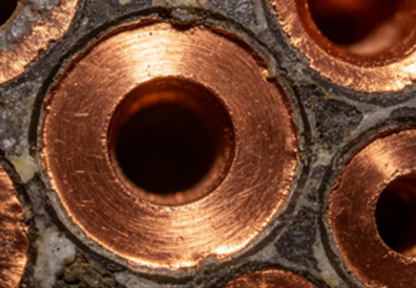
Plating processes also face limitations at higher ratios. Electrolytic copper deposition must achieve adequate throw into narrow, deep holes to ensure continuous coverage from top to bottom. Insufficient throwing power results in barrel plating that thins toward the center, creating potential failure points under thermal or mechanical stress. Laser drilling offers an alternative for microvias but is generally limited to shallower depths and is less common for full through-hole requirements in very thick constructions.
Material properties further influence outcomes. Resin systems with higher glass transition temperatures and controlled flow characteristics help maintain hole wall integrity during drilling. Copper foil thickness and inner layer registration tolerances also play roles, as misalignment can effectively increase the local aspect ratio encountered by the drill.
Practical Solutions and Best Practices
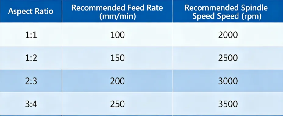
Design teams can mitigate aspect ratio challenges by selecting hole diameters that keep ratios within proven manufacturing windows, typically below 10:1 for standard mechanical drilling. When higher ratios are unavoidable, collaboration with fabricators during the design review stage helps identify feasible parameters. Specifying appropriate drill bit geometries, peck drilling cycles, and optimized feed rates improves chip removal and reduces heat buildup.
Process controls during plating include pulse plating techniques and careful selection of additives that enhance solution agitation inside high-aspect-ratio holes. Post-drill desmear and etchback steps must be calibrated to clean hole walls thoroughly without excessively enlarging the entrance or exit diameters. Quality verification often incorporates cross-section analysis and plating thickness measurements at multiple points along the barrel.
Advanced equipment such as high-speed spindles with precise depth control and automated optical inspection systems supports consistent results across production lots. Maintaining tight tolerances on stack-up thickness and using stable laminates further reduces variability that could push effective aspect ratios outside acceptable limits.
Key Considerations for High-Layer-Count Manufacturing
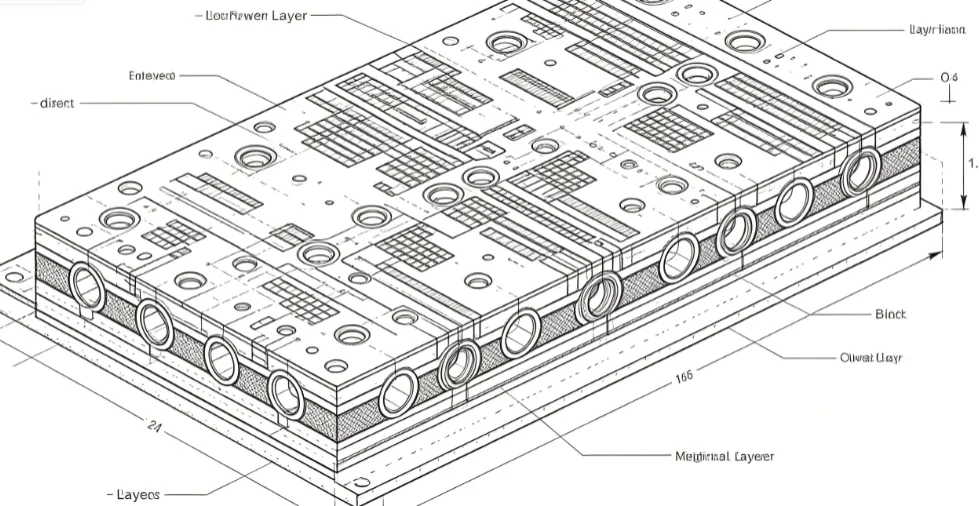
In practice, boards with 20 or more layers frequently exceed 2.5 mm in thickness. Maintaining registration across all layers becomes increasingly difficult, and any cumulative misalignment directly impacts the drilled hole path. Fabricators address this through sequential lamination or back-drilling strategies when stub lengths must be minimized for signal integrity reasons.
Thermal management during drilling also gains importance. Excessive heat can cause localized delamination or resin recession, particularly in boards using high-performance materials. Controlled drilling environments and periodic bit changes help sustain quality over long production runs.
Conclusion
Aspect ratio represents a fundamental constraint in high-layer-count PCB drilling that influences every subsequent process step. By understanding the interplay between board thickness, hole diameter, drilling mechanics, and plating dynamics, design and manufacturing teams can establish realistic targets that balance performance requirements with producibility. Early attention to this parameter, supported by adherence to established industry specifications, reduces risk and supports reliable outcomes in complex multilayer constructions.
FAQs
Q1: What is the typical maximum aspect ratio for mechanical drilling in high-layer-count PCBs?
A1: Mechanical drilling commonly accommodates aspect ratios up to approximately 10:1 in standard production environments. Higher ratios require specialized process adjustments or alternative via formation methods to maintain plating quality and hole integrity throughout the board thickness.
Q2: How does aspect ratio affect plating quality in multilayer PCB manufacturing?
A2: Higher aspect ratios make it more difficult for plating solutions to reach the center of the hole, potentially resulting in thinner copper deposits along the barrel. This can create reliability concerns under thermal cycling or current-carrying conditions if not properly controlled through process optimization.
Q3: Why is aspect ratio especially critical in high-layer-count PCB designs?
A3: Thicker boards required for high layer counts naturally increase the ratio when small via diameters are used for dense routing. This amplifies challenges in drilling debris removal, heat management, and achieving uniform plating, directly impacting yield and long-term board performance.
Q4: What design practices help manage PCB aspect ratio challenges?
A4: Engineers can select larger via diameters where routing density permits, collaborate with fabricators on stack-up thickness targets, and incorporate design rules that keep ratios within proven manufacturing capabilities. Early review of hole sizes against expected board thickness supports better outcomes.
References
IPC-6012E — Qualification and Performance Specification for Rigid Printed Boards. IPC, 2017
IPC-A-600K — Acceptability of Printed Boards. IPC, 2020