ALLPCB


Simulating Stackup Performance for Signal Integrity Before Fabrication
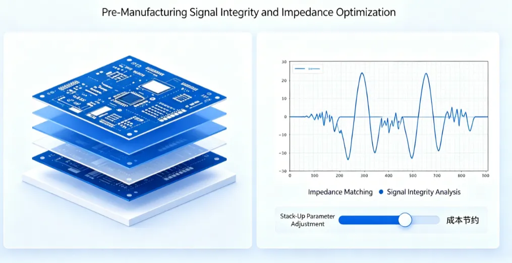
Engineers working on high-speed printed circuit boards face increasing demands for reliable signal transmission as data rates rise and board densities grow. Simulating the PCB stackup before fabrication allows designers to predict and optimize electrical performance without committing to physical prototypes. This approach identifies potential issues with impedance, propagation characteristics, and noise coupling early in the design cycle. By modeling the layer arrangement, dielectric materials, and trace geometries, teams can refine the configuration to meet target specifications. Such pre-layout analysis reduces the risk of costly revisions after boards are manufactured.
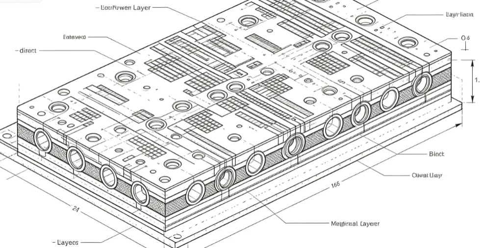
A well-planned stackup defines the vertical arrangement of copper layers and insulating materials that directly influence how signals travel across the board. Without simulation, assumptions about impedance or coupling may prove inaccurate once fabrication tolerances come into play. PCB stackup simulation provides quantitative feedback on parameters such as characteristic impedance and crosstalk levels before any material is ordered. This practice supports compliance with performance expectations in demanding applications like telecommunications and computing hardware. Early validation also helps procurement teams align material selections with achievable electrical outcomes.
Why PCB Stackup Simulation Matters for Signal Integrity
Signal integrity challenges often stem from mismatches between intended and actual stackup behavior. Variations in dielectric thickness or copper roughness can shift impedance outside acceptable windows. Simulation tools enable iterative adjustments to trace widths, spacings, and reference plane placements while the design remains flexible. Teams that incorporate these checks typically experience fewer post-fabrication test failures related to reflections or excessive noise. The process ultimately shortens development timelines by catching problems that would otherwise surface during prototype evaluation.
Technical Principles of Stackup and Signal Integrity Simulation
The foundation of stackup performance lies in the electromagnetic interactions between conductors and dielectrics. Characteristic impedance depends on the geometry of signal traces relative to their return paths and the permittivity of surrounding materials. Crosstalk arises when electric and magnetic fields from one trace induce unwanted voltages or currents in adjacent traces. Pre-layout simulation models these effects using two-dimensional or three-dimensional field solvers that solve Maxwell’s equations for the proposed configuration. Results guide refinements such as adjusting dielectric constants or adding ground planes to contain fields more effectively.
Propagation delay and loss characteristics also vary with stackup choices. Thicker dielectrics may lower capacitance but increase inductance, altering signal velocity. Frequency-dependent losses from conductor skin effect and dielectric dissipation become significant at higher data rates. Simulation accounts for these factors by incorporating material properties across the operating frequency range. Engineers can then compare multiple stackup options side by side to select the arrangement that balances impedance control with manufacturability. This structured evaluation follows logical steps of defining targets, modeling the geometry, running the solver, and interpreting the output metrics.
Crosstalk simulation specifically examines both near-end and far-end coupling coefficients between victim and aggressor nets. Differential pair configurations require careful symmetry in the stackup to maintain consistent impedance and minimize mode conversion. Reference plane continuity and via placement further influence return current paths that affect overall noise performance. By quantifying these interactions before layout completion, designers avoid routing decisions that would later prove problematic. The analysis integrates seamlessly with impedance calculations to produce a cohesive view of expected board behavior.
Best Practices for Effective Pre-Layout Stackup Simulation
Begin by establishing clear electrical targets derived from system requirements, including impedance tolerances and maximum allowable crosstalk. Select candidate stackups that respect standard layer counts and material availability while meeting those targets. Run simulations on representative trace configurations, including single-ended, differential, and bus structures that will appear in the final design. Review results for sensitivity to manufacturing tolerances such as etch factor or dielectric thickness variation. Iterate on the stackup until performance margins satisfy the specifications under worst-case conditions.
Document the simulation assumptions and outcomes to support design reviews and future revisions. Collaborate between electrical and mechanical teams to ensure the chosen arrangement also satisfies thermal and mechanical constraints. Validate key findings against physical test vehicles when possible, though the goal remains to minimize such builds. Consistent application of these steps leads to stackups that perform reliably once fabricated. Teams following this workflow report improved first-pass success rates on high-speed interfaces.
Maintain awareness of how stackup decisions interact with other design elements such as via structures and connector interfaces. Avoid over-constraining the stackup early; instead, allow flexibility for minor adjustments during layout. Use standardized reporting formats for simulation data so that results remain traceable and comparable across projects. These practices promote repeatable outcomes and facilitate knowledge transfer within engineering groups.
Conclusion
Pre-fabrication simulation of PCB stackup performance provides engineers with actionable insights into signal integrity before resources are committed to manufacturing. By modeling impedance, crosstalk, and related parameters, teams can optimize layer arrangements and material selections with confidence. The approach aligns with established engineering workflows that emphasize verification at each stage of development. Ultimately, this method supports the creation of boards that meet performance goals while controlling project costs and schedules.
FAQs
Q1: What is PCB stackup simulation and how does it support signal integrity?
A1: PCB stackup simulation models the layered structure of a printed circuit board to predict electrical behavior such as impedance and crosstalk before fabrication begins. It allows designers to evaluate how material choices and geometry affect signal transmission quality. By identifying mismatches early, engineers can adjust the configuration to achieve controlled impedance and reduced noise coupling. This process integrates with broader signal integrity analysis to improve overall board reliability.
Q2: How do signal integrity simulation tools evaluate pre-layout stackup options?
A2: Signal integrity simulation tools apply electromagnetic field calculations to proposed stackup geometries and material properties. They compute metrics including characteristic impedance, propagation delay, and coupling coefficients across relevant frequencies. Engineers compare multiple configurations to select the one that best satisfies target specifications. The results guide refinements without requiring physical prototypes.
Q3: Why perform impedance simulation PCB work prior to layout completion?
A3: Impedance simulation performed early reveals how trace dimensions and reference planes interact within a given stackup. It prevents routing decisions that would later violate impedance targets after fabrication tolerances are applied. Early analysis also supports consistent performance across single-ended and differential signals. This proactive step reduces the likelihood of redesign cycles.
Q4: What role does crosstalk simulation play in stackup optimization?
A4: Crosstalk simulation quantifies unwanted coupling between adjacent traces or pairs within the proposed stackup. It highlights the impact of spacing, plane placement, and dielectric properties on noise levels. Designers use these insights to adjust geometries or add shielding features that maintain signal fidelity. Effective crosstalk control contributes directly to meeting system-level noise budgets.
References
IPC-2221B — Generic Standard on Printed Board Design. IPC, 2012
IPC-6012E — Qualification and Performance Specification for Rigid Printed Boards. IPC, 2017
IPC-2141A — Controlled Impedance Circuit Boards and High Speed Logic Design. IPC, 2004