ALLPCB


Building a cloud server at home is an exciting way to create a powerful, custom setup for personal projects or small-scale hosting. With DIY server PCB projects, hobbyists can design a home lab motherboard tailored to their needs using custom PCB design techniques. In this guide, we’ll walk you through the process of creating low-cost server PCB solutions for your home lab, from planning to execution, with practical tips for hobbyist PCB projects.
Whether you’re looking to save costs or gain hands-on experience, designing a custom motherboard for a home server is a rewarding challenge. This blog dives deep into the essentials of DIY server PCB projects, offering step-by-step guidance, technical insights, and low-cost strategies to help you succeed. Let’s get started on building your very own home lab motherboard!
Why Build a DIY Server PCB for Your Home Lab?
Setting up a cloud server at home gives you full control over data, performance, and customization. While pre-built servers are convenient, they often come with high costs and limited flexibility. A DIY server PCB project lets you create a home lab motherboard that matches your exact specifications, whether it’s for storage, virtualization, or hosting personal applications.
Here are some key benefits of pursuing hobbyist PCB projects for home labs:
- Cost Savings: Building a custom PCB design can be much cheaper than buying commercial server hardware, especially with low-cost server PCB manufacturing options.
- Learning Opportunity: Designing a motherboard teaches valuable skills in electronics, circuit design, and PCB layout.
- Customization: Tailor your server to specific needs, like high-speed data transfer or energy efficiency, by controlling every aspect of the design.
Getting Started with DIY Server PCB Projects
Before diving into custom PCB design, it’s important to understand the basics of what goes into a home lab motherboard. A server PCB needs to handle multiple components like processors, memory modules, storage interfaces, and network connections. For hobbyists, starting small and scaling up is often the best approach.
1. Define Your Home Lab Needs
First, decide what your cloud server will do. Are you hosting a personal website, running virtual machines, or creating a network-attached storage (NAS) system? Your goals will shape the design of your DIY server PCB. For example:
- A NAS server might prioritize multiple SATA connections for hard drives.
- A virtualization server could need support for high RAM capacity and multi-core processors.
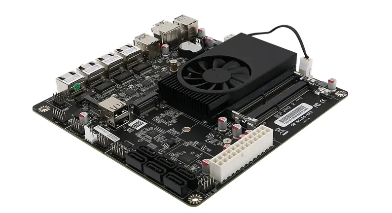
2. Choose the Right Components
Selecting components is a critical step in hobbyist PCB projects. Focus on compatibility and performance. Common components for a home lab motherboard include:
- Processor Socket: Choose a socket type that supports affordable, server-grade CPUs. For instance, an AM4 socket works with many budget-friendly processors suitable for home labs.
- Memory Slots: Opt for DDR4 slots if you’re aiming for a low-cost server PCB, as they balance cost and performance.
- Storage Interfaces: Include SATA or NVMe slots for fast storage options.
- Network Ports: Gigabit Ethernet ports are essential for a cloud server to ensure fast data transfer speeds (up to 1000 Mbps).
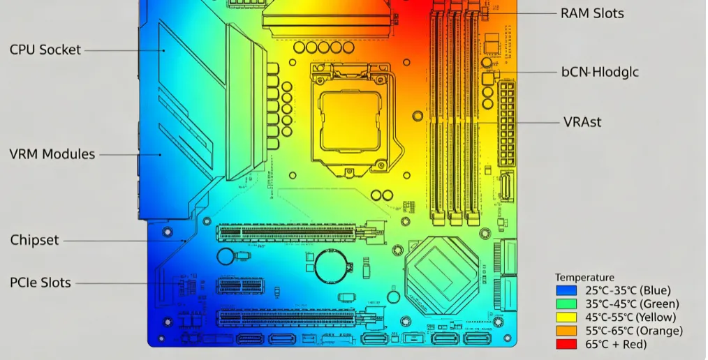
Designing Your Custom PCB for a Home Lab Motherboard
Creating a custom PCB design for a server requires careful planning and attention to detail. Here’s a step-by-step guide to help you through the process of designing a home lab motherboard.
1. Schematic Design
Start by creating a schematic that maps out how components connect. Use design software to draw the electrical connections between the CPU, memory, power supply, and other parts. Pay attention to signal integrity, ensuring that high-speed signals (like PCIe lanes operating at 8 GT/s) aren’t interfered with by nearby traces.
2. PCB Layout
Once the schematic is ready, move to the PCB layout. This step involves placing components on the board and routing traces. Keep these tips in mind for a successful custom PCB design:
- Layer Stackup: For a server PCB, use at least 4 layers. Dedicate two layers to power and ground planes to reduce noise and maintain impedance (typically around 50 ohms for high-speed signals).
- Trace Width: For power traces, use wider paths (e.g., 20-30 mils) to handle higher currents, while signal traces can be narrower (around 6-8 mils).
- Component Placement: Place high-speed components like the CPU and RAM closer together to minimize signal delay.
3. Power Delivery and Cooling
A home lab motherboard needs a robust power delivery system. Design voltage regulator modules (VRMs) to supply stable power (e.g., 1.2V for CPU cores) and prevent overheating. Add mounting points for heatsinks or fans near the CPU and power components to manage thermal output.
Low-Cost Server PCB Manufacturing Tips
For hobbyist PCB projects, keeping costs down is often a priority. Here are some strategies to create a low-cost server PCB without sacrificing quality.
1. Optimize Board Size
Smaller boards are cheaper to produce. Design your home lab motherboard to fit within standard panel sizes (like 100mm x 100mm) to avoid extra manufacturing fees. If your design is compact, you can often fit multiple boards on a single panel, further reducing costs.
2. Use Standard Materials
Stick to common PCB materials like FR-4, which is widely available and affordable. Avoid exotic materials unless your server requires high-frequency performance (above 5 GHz), which is rare for most home lab setups.
3. Batch Production
If you’re confident in your design, order multiple copies of your PCB at once. Many manufacturing services offer discounts for larger quantities, making each board cheaper overall. For example, producing 5 boards might cost $2 per board, while a single board could cost $5.
Image Placement Suggestion: Place an image of a stack of manufactured PCBs ready for assembly. ALT Text: "Low-cost server PCB batch production"
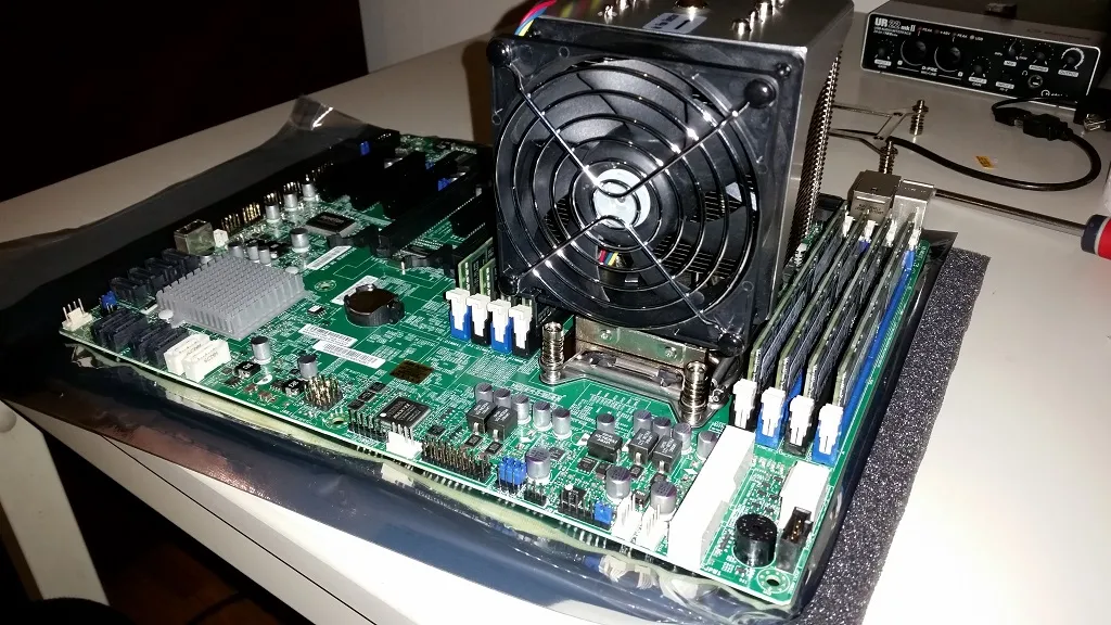
Assembling and Testing Your DIY Server PCB
Once your custom PCB design is manufactured, it’s time to assemble and test your home lab motherboard. Follow these steps to ensure everything works as planned.
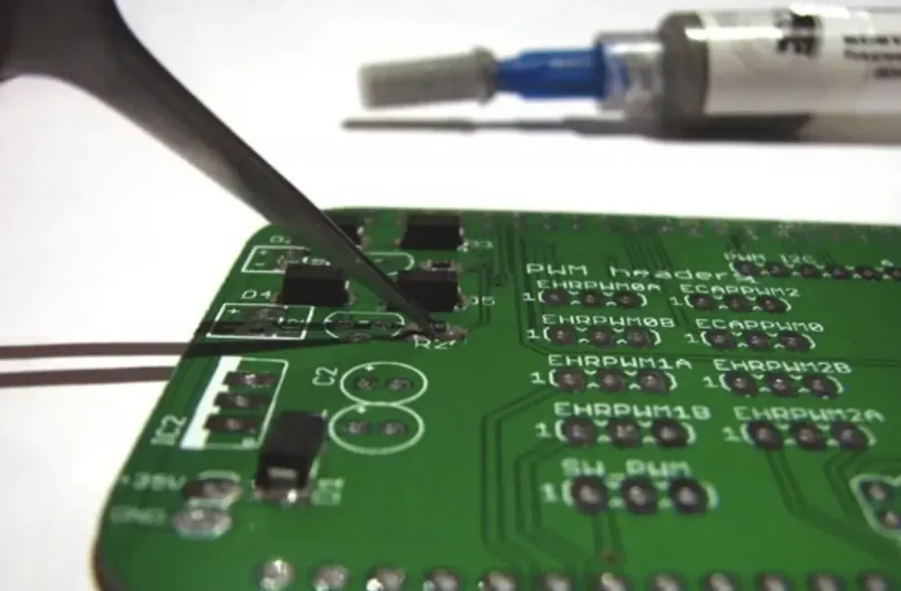
1. Soldering Components
Carefully solder components onto the board, starting with smaller parts like resistors and capacitors before moving to larger ones like the CPU socket. Use a soldering iron with a fine tip (around 1mm) and set it to a temperature of about 300°C for lead-free solder.
2. Power-On Test
Before fully assembling the server, perform a power-on test. Connect a power supply (e.g., a 24-pin ATX connector delivering 12V and 5V rails) and check for basic functionality. Use a multimeter to verify voltages at key points, ensuring they match expected values (e.g., 3.3V for memory).
3. Debugging Issues
If the board doesn’t work, check for common issues like cold solder joints or incorrect component placement. Inspect high-speed signal lines for noise using an oscilloscope if available, ensuring signal rise times are within acceptable limits (e.g., under 1 ns for PCIe).
Scaling Up Your Home Lab Motherboard Project
Once your initial DIY server PCB is functional, consider scaling up for more advanced features. Add support for multiple network ports (e.g., dual Gigabit Ethernet) or upgrade to faster storage interfaces like PCIe 4.0, which offers speeds up to 16 GB/s for NVMe drives. Each iteration of your custom PCB design will improve your skills and result in a more capable home lab motherboard.
Common Challenges in Hobbyist PCB Projects
Building a DIY server PCB isn’t without hurdles. Here are some common challenges and how to overcome them:
- Signal Interference: High-speed signals can interfere with each other if traces are too close. Maintain at least 3x the trace width as spacing between critical lines.
- Thermal Management: Servers generate heat. Ensure adequate cooling by designing space for fans or heatsinks, especially around components drawing over 50W.
- Component Sourcing: Some server-grade parts can be expensive or hard to find. Look for second-hand components or compatible alternatives to keep costs low.
Final Thoughts on DIY Server PCB for Home Labs
Creating a cloud server at home with a DIY server PCB is a fantastic way to dive into custom PCB design while building something practical for your home lab. By focusing on a well-planned home lab motherboard, using low-cost server PCB strategies, and learning through hobbyist PCB projects, you can achieve professional-grade results on a budget.
The journey of designing and assembling a custom motherboard teaches invaluable skills and offers endless possibilities for customization. Start small, test often, and don’t be afraid to iterate on your designs. With the right approach, your home lab can become a powerful hub for all your computing needs. Take the first step today and bring your cloud server vision to life!