 ALLPCB


In the fast-paced world of gaming, next-gen consoles demand cutting-edge technology to deliver seamless graphics, lightning-fast response times, and immersive experiences. At the heart of these powerful machines lies the printed circuit board (PCB), a critical component that can make or break performance. So, how do you optimize PCB design for gaming consoles to achieve peak performance? By focusing on high-speed PCB layout, signal integrity, thermal management, low-latency design, and an effective PCB stack-up, you can ensure that gaming hardware meets the demands of modern gamers.
In this comprehensive guide, we’ll dive deep into the essentials of PCB design tailored for gaming consoles. Whether you’re an engineer working on the next big console or a designer looking to understand the intricacies of gaming hardware, this post will walk you through actionable strategies and technical insights to elevate your designs. Let’s explore how to unlock the full potential of next-gen gaming technology.
Why PCB Design Matters for Next-Gen Gaming Consoles
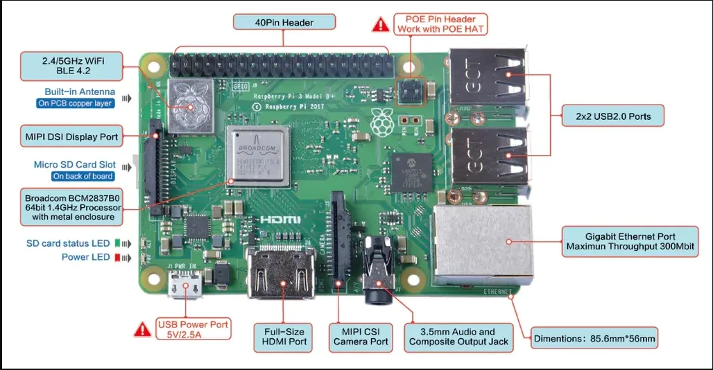
Gaming consoles are no longer just entertainment devices; they are high-performance computing systems packed into compact designs. From rendering 4K graphics at 120 frames per second to supporting real-time ray tracing, these systems push hardware to the limit. The PCB serves as the foundation, connecting processors, GPUs, memory, and other components while ensuring flawless communication and power delivery.
A poorly designed PCB can lead to signal delays, overheating, and electromagnetic interference (EMI), all of which degrade gaming performance. On the other hand, an optimized PCB enhances speed, reduces latency, and maintains stability even under heavy workloads. By focusing on key design aspects like high-speed PCB layout for gaming consoles and signal integrity PCB design, manufacturers can create hardware that stands up to the rigorous demands of modern gaming.
Key Elements of High-Speed PCB Layout for Gaming Consoles
High-speed PCB layout is critical for gaming consoles where data transfer rates between components often exceed several gigabits per second. A well-executed layout minimizes signal loss and ensures that high-frequency signals travel without distortion. Here are some core principles to follow for a high-speed PCB layout in gaming consoles:
- Trace Length Matching: When dealing with high-speed signals like DDR4 memory or PCIe lanes (common in gaming hardware), ensure that trace lengths are matched to avoid timing skews. For instance, a mismatch of just 1 millimeter in trace length can introduce a delay of about 6 picoseconds, which is significant at multi-GHz speeds.
- Impedance Control: Maintain consistent impedance (typically 50 ohms for single-ended signals and 100 ohms for differential pairs) across traces to prevent reflections. Use controlled dielectric materials and precise trace widths to achieve this.
- Minimize Crosstalk: Place high-speed traces apart from each other or use ground planes to shield signals. Crosstalk can introduce noise, impacting data integrity in critical paths like GPU-to-memory communication.
- Via Optimization: Excessive vias in high-speed paths can cause signal degradation. Use back-drilling techniques to remove unused via stubs and reduce parasitic capacitance.
By adhering to these guidelines, designers can ensure that data flows smoothly between components, enabling consoles to handle intensive tasks without bottlenecks.
Ensuring Signal Integrity in PCB Design for Gaming Hardware
Signal integrity (SI) is the cornerstone of reliable performance in gaming consoles. Poor SI can lead to data corruption, jitter, and system crashes—issues that no gamer wants to face. Focusing on signal integrity PCB design involves addressing several factors:
- Power Delivery Network (PDN): A robust PDN ensures stable voltage levels for high-speed components. Use multiple decoupling capacitors near power pins to suppress noise. For example, a GPU operating at 1.2V might require a ripple of less than 50mV to function reliably.
- Grounding Strategy: Implement a solid ground plane to provide a low-impedance return path for signals. Split ground planes can cause EMI issues, so maintain a continuous ground layer wherever possible.
- Termination Techniques: Use proper termination resistors for high-speed interfaces like HDMI or USB-C, which are common in gaming consoles. This prevents signal reflections that could corrupt data.
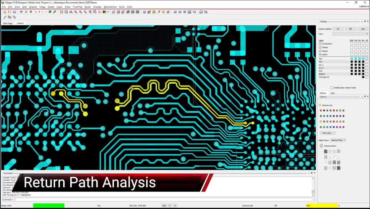
- Simulation and Testing: Leverage SI simulation tools to model signal behavior before fabrication. These tools can predict issues like overshoot or ringing, allowing for design adjustments early in the process.
Maintaining signal integrity ensures that every command, from a button press to a complex rendering task, is executed without errors, providing gamers with a seamless experience.
Thermal Management in Gaming PCBs: Keeping It Cool Under Pressure
Gaming consoles generate significant heat due to powerful processors and GPUs running at full throttle. Effective thermal management for gaming PCBs is essential to prevent thermal throttling and extend hardware lifespan. Here’s how to tackle heat in PCB design:
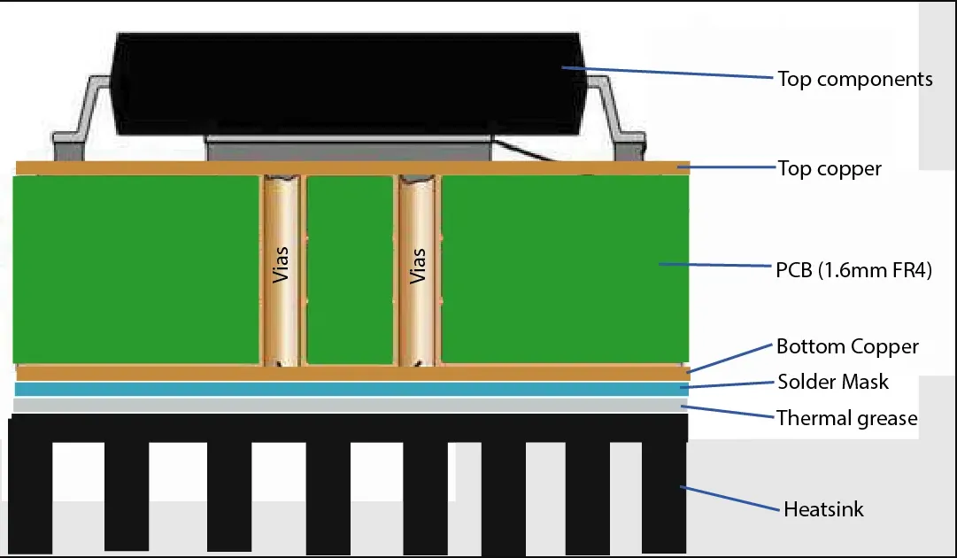
- Heat Sink Integration: Place heat sinks or thermal pads directly over high-power components like CPUs and GPUs. Ensure that the PCB layout allows for proper mounting and airflow around these areas.
- Thermal Vias: Use arrays of thermal vias under hot components to transfer heat to inner copper layers or external heat sinks. For instance, a grid of 0.3mm vias with 1.2mm spacing can significantly improve heat dissipation.
- Copper Pour for Heat Spreading: Increase copper thickness (e.g., 2oz or more) in power delivery areas to spread heat evenly across the board. This is particularly useful for voltage regulator modules (VRMs) in gaming hardware.
- Component Placement: Position heat-generating components away from sensitive areas like memory modules. Also, align them with the console’s cooling system, such as fans or vents, for maximum efficiency.
Proper thermal management ensures that gaming consoles run at peak performance without overheating, even during marathon gaming sessions.
Designing Low-Latency PCBs for Real-Time Gaming
Latency is the enemy of competitive gaming, where every millisecond counts. A low-latency PCB design minimizes delays in signal transmission, ensuring that player inputs are processed instantly. Here are key strategies to achieve this:
- Short Signal Paths: Reduce the physical distance between critical components like the controller input circuitry and the main processor. Shorter paths mean faster signal travel—crucial for real-time response.
- High-Speed Materials: Use low-loss dielectric materials with a dielectric constant (Dk) of around 3.0 to 3.5 for high-speed signals. These materials reduce signal delay compared to standard FR-4 substrates (Dk ~4.5).
- Optimized Clock Distribution: Ensure that clock signals, which synchronize data transfer, are routed with minimal skew. A delay of just 10 picoseconds in a clock signal can disrupt timing in a high-speed system.
- Reduce Parasitic Effects: Minimize parasitic capacitance and inductance in traces and vias, as these can slow down signal propagation and increase latency.
By prioritizing low-latency design, PCB engineers can help create gaming consoles that respond instantly to player actions, giving gamers a competitive edge.
Mastering Gaming Console PCB Stack-Up for Performance and Reliability
The PCB stack-up, or the arrangement of copper and insulating layers, plays a vital role in performance, signal integrity, and thermal management. A well-designed gaming console PCB stack-up balances these factors while keeping manufacturing costs in check. Here’s how to approach stack-up design:
- Layer Count: Gaming console PCBs often use 6 to 12 layers to accommodate complex routing and power distribution. For example, a 10-layer stack-up might include 4 signal layers, 4 ground/power planes, and 2 outer layers for components.
- Power and Ground Planes: Place power and ground planes adjacent to each other to create a low-inductance path for current return. This reduces noise and improves signal integrity.
- Signal Layer Placement: Route high-speed signals on inner layers sandwiched between ground planes to shield them from external interference. For instance, PCIe or DDR signals should be routed on internal layers for maximum protection.
- Material Selection: Choose materials with consistent dielectric properties across layers to maintain signal speed and impedance. High-frequency laminates are often used for critical layers in gaming PCBs.
A thoughtfully designed stack-up ensures that all aspects of the PCB—signal integrity, power delivery, and thermal performance—work in harmony to support the demands of next-gen gaming consoles.
Practical Tips for Optimizing PCB Design in Gaming Consoles
Beyond the technical aspects, here are some practical tips to streamline the design process and achieve optimal results:
- Collaborate Early: Work closely with hardware engineers, firmware developers, and thermal specialists during the design phase to address potential issues before they arise.
- Iterate with Prototypes: Build and test multiple prototypes to validate design choices. Real-world testing can reveal issues like EMI or thermal hotspots that simulations might miss.
- Stay Updated on Standards: Keep up with industry standards like IPC-2221 for PCB design and manufacturing. Compliance ensures reliability and compatibility with modern components.
- Leverage Advanced Tools: Use design software with built-in SI and thermal analysis features to simulate performance under various conditions. This can save time and reduce costly redesigns.
These steps help ensure that the final PCB design is not only high-performing but also manufacturable and cost-effective.
Conclusion: Building the Future of Gaming with Optimized PCB Design
Next-gen gaming consoles are marvels of engineering, and their performance hinges on the quality of PCB design. By focusing on high-speed PCB layout for gaming consoles, signal integrity PCB design, thermal management for gaming PCBs, low-latency PCB strategies, and a robust gaming console PCB stack-up, designers can create hardware that delivers unparalleled gaming experiences.
At ALLPCB, we understand the challenges of designing PCBs for cutting-edge applications like gaming consoles. Our expertise in high-speed design, advanced materials, and precision manufacturing can help bring your vision to life. Whether you’re tackling signal integrity issues or optimizing thermal performance, we’re here to support you every step of the way. Let’s build the future of gaming together with PCB designs that push the boundaries of performance.


