 ALLPCB


If you're a PCB designer looking to enhance the performance and reliability of your boards, especially for high-speed applications, you've likely come across ENEPIG. But what is ENEPIG, and how can it benefit your designs? ENEPIG, or Electroless Nickel Electroless Palladium Immersion Gold, is a surface finish for printed circuit boards (PCBs) that offers superior corrosion resistance, excellent solderability, and compatibility with wire bonding. In this comprehensive guide, we’ll dive deep into ENEPIG PCB design rules, ENEPIG layer thickness, ENEPIG impedance control, high-speed PCB ENEPIG, and ENEPIG signal integrity to help you unlock its full potential for your projects.
Whether you're designing for consumer electronics, automotive systems, or telecommunications, understanding how to leverage ENEPIG can make a significant difference. Let’s explore everything you need to know to integrate this powerful surface finish into your PCB designs.
What is ENEPIG and Why Should PCB Designers Care?
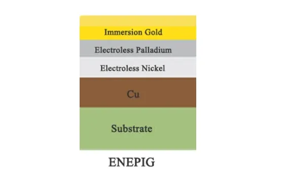
ENEPIG stands for Electroless Nickel Electroless Palladium Immersion Gold, a multi-layer surface finish applied to the copper pads of a PCB. This finish consists of three layers: a nickel base layer for corrosion resistance, a palladium middle layer for additional protection and wire bonding compatibility, and a thin gold top layer for excellent solderability and conductivity.
Why should you care about ENEPIG as a PCB designer? This finish is particularly valuable for applications requiring high reliability and performance. It prevents issues like "black pad" (a defect seen in other finishes like ENIG) and supports both soldering and wire bonding, making it ideal for complex designs. Additionally, ENEPIG is well-suited for high-speed and high-frequency applications due to its minimal impact on signal integrity, a critical factor for modern electronics.
In the sections below, we’ll break down the specific design considerations and benefits of using ENEPIG, ensuring you have actionable insights to apply to your next project.
ENEPIG PCB Design Rules: Key Guidelines for Success
When incorporating ENEPIG into your PCB design, following specific design rules is essential to maximize its benefits. These guidelines ensure compatibility with manufacturing processes and help maintain the integrity of your board.
- Pad Size and Spacing: ENEPIG works best with standard pad sizes and spacing. Ensure that your design adheres to minimum spacing requirements to avoid issues during the plating process. For fine-pitch components, aim for a pad-to-pad spacing of at least 0.2 mm to prevent bridging during soldering.
- Via and Hole Considerations: For plated through-holes (PTH), ensure that the aspect ratio (hole depth to diameter) does not exceed 10:1, as higher ratios can lead to uneven plating of the ENEPIG layers, affecting reliability.
- Surface Finish Compatibility: ENEPIG is compatible with most PCB materials, but confirm with your fabrication partner that your chosen substrate and laminate materials support this finish, especially for high-frequency designs.
- Thermal Management: Since ENEPIG involves a nickel layer, which has lower thermal conductivity than copper, consider thermal vias or heat sinks in areas with high heat dissipation to prevent overheating during operation.
By adhering to these ENEPIG PCB design rules, you can avoid common pitfalls and ensure a smooth manufacturing process, resulting in a high-quality final product.
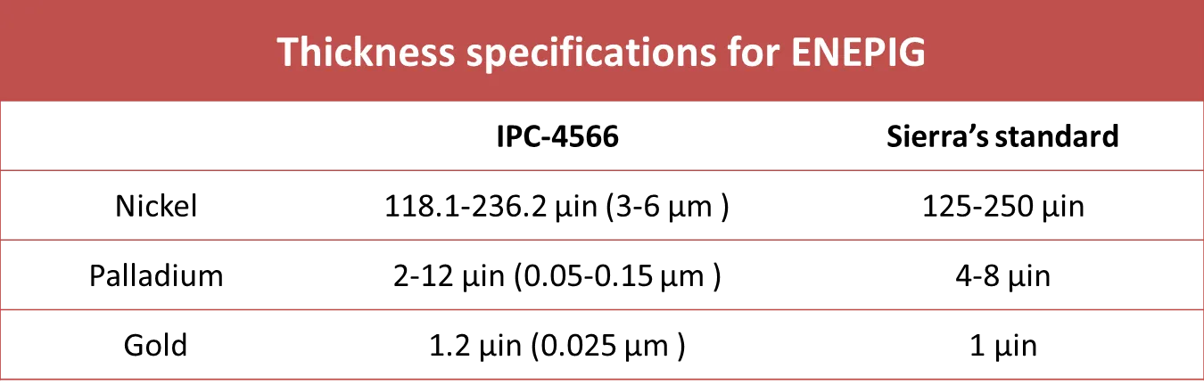
ENEPIG Layer Thickness: Striking the Right Balance
The thickness of each layer in an ENEPIG finish plays a critical role in its performance. Each layer—nickel, palladium, and gold—has a specific purpose, and their thicknesses must be carefully controlled to meet industry standards and application needs.
- Nickel Layer: Typically, the nickel layer ranges from 3 to 6 micrometers (μm). This layer acts as a barrier to prevent copper diffusion and provides corrosion resistance. A thickness below 3 μm may compromise protection, while exceeding 6 μm can introduce unnecessary stress on the PCB.
- Palladium Layer: The palladium layer is usually between 0.05 and 0.3 μm. This thin layer enhances wire bonding capabilities and prevents nickel oxidation. Keeping it within this range ensures cost-effectiveness without sacrificing performance.
- Gold Layer: The top gold layer is often the thinnest, ranging from 0.03 to 0.1 μm. This layer ensures excellent solderability and conductivity. A thicker gold layer can increase costs without significant benefits, while a thinner layer may wear off during handling or soldering.
Understanding ENEPIG layer thickness is crucial for optimizing both cost and performance. Work closely with your PCB manufacturer to specify these thicknesses based on your project’s requirements, such as whether the board will undergo multiple soldering cycles or needs enhanced wire bonding capabilities.
ENEPIG Impedance Control: Ensuring Consistency in High-Speed Designs
For high-speed and high-frequency PCB designs, maintaining consistent impedance is critical to prevent signal loss and interference. ENEPIG impedance control is an important consideration because the surface finish can subtly affect the electrical properties of the traces and pads.
ENEPIG itself does not significantly alter the characteristic impedance of traces compared to other finishes like ENIG (Electroless Nickel Immersion Gold). However, the nickel layer in ENEPIG can introduce a slight increase in skin effect losses at very high frequencies (above 10 GHz) due to its magnetic properties. To mitigate this:
- Trace Width and Spacing: Design your traces to achieve the target impedance (e.g., 50 ohms for single-ended signals or 100 ohms for differential pairs) using standard impedance calculators. Ensure that the dielectric material and trace geometry account for any minor variations introduced by the surface finish.
- Ground Planes: Use continuous ground planes beneath high-speed signal traces to minimize impedance mismatches. Avoid large cutouts or splits in the ground plane near critical signals.
- Simulation Tools: Employ PCB simulation software to model the impact of ENEPIG on impedance, especially for frequencies above 5 GHz, where even small variations can affect performance.
By focusing on these aspects, you can achieve precise ENEPIG impedance control, ensuring your high-speed designs operate without unexpected signal degradation.
High-Speed PCB ENEPIG: Optimizing for Performance
High-speed PCB ENEPIG applications are increasingly common in industries like telecommunications, data centers, and automotive electronics, where signal speeds often exceed 10 Gbps. ENEPIG is an excellent choice for these designs due to its low signal loss and compatibility with fine-pitch components.
Here are some key tips for optimizing ENEPIG in high-speed PCB designs:
- Minimize Signal Loss: The thin gold layer in ENEPIG ensures low contact resistance, which is vital for high-speed signals. Pair this with low-loss dielectric materials (e.g., with a dielectric constant, Dk, below 3.5) to further reduce signal attenuation.
- Support for Fine-Pitch Components: ENEPIG’s excellent solderability supports the use of fine-pitch components like BGAs (Ball Grid Arrays) with pitches as low as 0.4 mm, common in high-speed designs.
- Thermal Stability: High-speed circuits often generate heat. ENEPIG’s robust nickel layer provides thermal stability, but ensure your design includes adequate heat dissipation strategies to prevent performance issues.
By leveraging these strategies, ENEPIG can help you achieve top-tier performance in high-speed PCB ENEPIG designs, meeting the demands of modern electronics.
ENEPIG Signal Integrity: Maintaining Clean and Reliable Signals
Signal integrity is the cornerstone of any high-performance PCB, and ENEPIG signal integrity benefits are a major reason designers choose this finish. Poor signal integrity can lead to data errors, crosstalk, and electromagnetic interference (EMI), all of which can cripple a design.
ENEPIG contributes to signal integrity in several ways:
- Low Contact Resistance: The gold layer ensures minimal contact resistance at solder joints and connectors, reducing signal distortion.
- Reduced Crosstalk: Proper impedance control and grounding techniques, combined with ENEPIG’s consistent surface properties, help minimize crosstalk between adjacent traces, even at high frequencies.
- Compatibility with High-Frequency Signals: Unlike some finishes that degrade at high frequencies, ENEPIG maintains signal quality, making it suitable for applications like 5G and IoT devices operating at frequencies up to 20 GHz or higher.
To maximize ENEPIG signal integrity, consider the following best practices:
- Route high-speed signals away from noisy power lines or switching components.
- Use differential pair routing for critical signals to maintain consistent impedance and reduce noise.
- Implement proper termination techniques (e.g., series or parallel termination) to prevent signal reflections.
By combining ENEPIG with sound design practices, you can ensure clean, reliable signals across your PCB, even in the most demanding applications.
Advantages of ENEPIG Over Other Surface Finishes
ENEPIG stands out among other PCB surface finishes due to its unique combination of benefits. Here’s how it compares to alternatives like HASL (Hot Air Solder Leveling) and ENIG:
- Versatility: Unlike HASL, which is unsuitable for fine-pitch components, ENEPIG supports both soldering and wire bonding, making it ideal for mixed-technology boards.
- Reliability: Compared to ENIG, ENEPIG eliminates the risk of "black pad" defects due to the palladium layer, ensuring better long-term reliability.
- Performance: ENEPIG’s thin gold layer provides better conductivity and signal performance than thicker finishes, which can introduce parasitic capacitance or inductance.
While ENEPIG may come at a slightly higher cost than some alternatives, its advantages in reliability and performance often justify the investment, especially for high-stakes applications.
Practical Applications of ENEPIG in PCB Design
ENEPIG is widely used across various industries due to its robust properties. Some common applications include:
- Telecommunications: High-speed routers and switches benefit from ENEPIG’s signal integrity and impedance control, supporting data rates above 25 Gbps.
- Automotive: In advanced driver-assistance systems (ADAS), ENEPIG ensures reliability under harsh environmental conditions, withstanding temperature cycles from -40°C to 125°C.
- Medical Devices: For implantable or wearable devices, ENEPIG’s corrosion resistance and biocompatibility make it a trusted choice.
These real-world examples highlight how ENEPIG can address the specific challenges of diverse industries, providing designers with a versatile and reliable surface finish.
Conclusion: Elevate Your PCB Designs with ENEPIG
ENEPIG is a game-changer for PCB designers seeking to balance performance, reliability, and manufacturability. By understanding and applying ENEPIG PCB design rules, optimizing ENEPIG layer thickness, ensuring ENEPIG impedance control, leveraging benefits for high-speed PCB ENEPIG designs, and prioritizing ENEPIG signal integrity, you can create boards that meet the demands of today’s cutting-edge applications.
At ALLPCB, we’re committed to helping you achieve the best results for your projects. Whether you’re designing for high-speed data transmission or harsh environmental conditions, ENEPIG offers the versatility and performance you need. Incorporate these insights into your next design, and unlock the full power of this advanced surface finish to take your PCBs to the next level.


