 ALLPCB


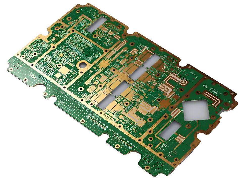
If you're diving into PCB design or circuit board assembly, you might be wondering about the solder mask layer in PCBs and how to optimize it for manufacturing. Simply put, the solder mask is a protective layer on a printed circuit board (PCB) that covers copper traces, preventing short circuits and oxidation while guiding solder during assembly. To ensure a flawless production process, following Design for Manufacturability (DFM) guidelines is crucial. In this blog, we'll explore the role of the solder mask, also known as solder resist, and share the top 4 DFM guidelines to help you create reliable and efficient PCB designs.
What Is the Solder Mask Layer in PCBs?
The solder mask layer in PCBs is a thin, protective coating applied over the copper traces and pads of a circuit board. Often made of a polymer material, this layer—commonly green but available in other colors like blue, red, or black—serves multiple purposes. It insulates the copper traces to prevent accidental short circuits, protects against environmental damage like oxidation, and ensures that solder only adheres to designated areas during assembly.
Without a proper solder mask, you risk issues like solder bridges (unwanted connections between pads) or corrosion of exposed copper, which can lead to board failure. For engineers and designers, understanding how to design this layer correctly is a key step in ensuring the manufacturability and longevity of a PCB.
Why Is Solder Mask Important in Circuit Board Assembly?
In circuit board assembly, the solder mask plays a critical role in maintaining precision and reliability. During the soldering process, whether it's wave soldering or reflow soldering, the solder mask ensures that molten solder only flows to the intended areas, such as component pads. This prevents solder from spreading to nearby traces, which could cause short circuits.
Additionally, the solder mask acts as a barrier against environmental factors. For instance, it protects copper traces from moisture, dust, and chemical exposure, which can degrade the board over time. In high-density designs, where components and traces are packed closely together, a well-designed solder mask is even more essential to avoid errors during assembly.
Key Challenges with Solder Mask in PCB Design
Designing the solder mask layer isn't without its challenges. Common issues include misalignment of the mask, insufficient clearance between pads and mask openings, or incomplete coverage over vias (known as via tenting). These problems can lead to manufacturing defects, such as exposed copper or solder bridging, which compromise the board's functionality.
For example, if the solder mask opening is too large, excess solder might accumulate on a pad, creating uneven connections. Conversely, if the opening is too small, it could restrict solder flow, leading to poor component attachment. Addressing these challenges through proper DFM guidelines is vital for a smooth manufacturing process.
Top 4 DFM Guidelines for Solder Mask Design in PCBs
To help you achieve a manufacturable and reliable PCB design, we've compiled the top 4 DFM guidelines for the solder mask layer. These tips are tailored for engineers working on circuit board assembly and focus on practical steps to minimize defects and optimize production.
1. Maintain Proper Solder Mask Clearances
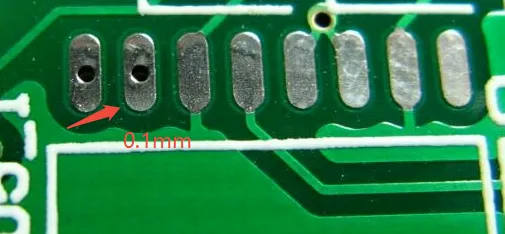
One of the most critical aspects of solder mask design is ensuring adequate clearance between the mask and the copper pads or traces. Clearance refers to the distance between the edge of the solder mask opening and the edge of the pad. If this clearance is too small, the mask might overlap the pad, reducing the area available for soldering. If it's too large, it risks exposing adjacent traces, leading to potential shorts.
As a general rule, aim for a solder mask clearance of at least 0.1 mm (4 mils) around each pad. For high-density designs, consult with your manufacturing partner to confirm their minimum clearance capabilities, as some advanced processes might allow for tighter tolerances. Properly defined clearances ensure that the solder adheres only to the intended areas during assembly, reducing the risk of defects.
2. Use Appropriate Via Tenting for Protection
Vias are small holes in a PCB that connect different layers of copper traces. If left uncovered, vias can attract solder during assembly, leading to unintended connections or reduced solder availability for nearby components. Via tenting refers to covering these holes with solder mask to prevent such issues.
For most designs, tenting vias on both the top and bottom sides is recommended, especially for smaller vias (less than 0.3 mm in diameter). However, for larger vias or those used for heat dissipation, leaving them partially exposed might be necessary. Be sure to specify your intent in the design files, as incomplete tenting can lead to manufacturing errors. Proper via tenting not only improves assembly outcomes but also enhances the board's resistance to environmental damage.
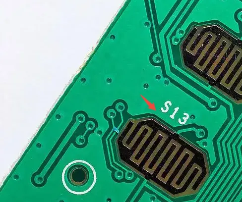
3. Avoid Solder Mask on Silkscreen Areas
The silkscreen layer on a PCB contains printed text and symbols, such as component labels or reference designators, to aid in assembly and troubleshooting. If the solder mask overlaps with silkscreen areas, it can obscure important markings, making the board difficult to read. This overlap often happens when the mask design isn't aligned correctly with the silkscreen layer.
To prevent this, ensure that solder mask openings do not extend into silkscreen areas. Most design software allows you to define a keep-out zone for the solder mask around silkscreen elements. A minimum separation of 0.2 mm (8 mils) between the solder mask edge and silkscreen text is a good starting point. This practice ensures clarity and avoids confusion during assembly or inspection.
4. Choose the Right Solder Mask Type and Thickness
Not all solder masks are created equal. The type and thickness of the solder mask can significantly impact the board's performance and manufacturability. Common types include liquid photoimageable (LPI) solder mask, which offers high precision for fine-pitch designs, and dry film solder mask, which is more suited for simpler boards.
The thickness of the solder mask also matters. A typical thickness ranges from 0.02 mm to 0.03 mm (0.8 to 1.2 mils) above the copper traces. If the mask is too thin, it might not provide adequate protection against environmental factors. If it's too thick, it can interfere with component placement or soldering. For high-frequency designs, consider a thinner mask to minimize dielectric effects that could impact signal integrity, especially if your board operates at frequencies above 1 GHz.
Work closely with your manufacturing team to select the appropriate solder mask type and thickness based on your design requirements. This collaboration ensures compatibility with their processes and helps avoid delays or rework.
Benefits of Following DFM Guidelines for Solder Mask Design
Adhering to DFM guidelines for the solder mask layer in PCBs offers several advantages. First, it reduces the likelihood of manufacturing defects, saving time and cost during production. For instance, proper clearances and via tenting can decrease the rejection rate of boards due to solder bridging by up to 30%, depending on the complexity of the design.
Second, a well-designed solder mask enhances the reliability of the final product. By protecting copper traces and ensuring precise soldering, the board is less prone to failures in the field, which is especially important for applications in harsh environments like automotive or industrial systems.
Finally, following these guidelines streamlines communication with your manufacturing partner. Clear, manufacturable designs minimize back-and-forth revisions, speeding up the time to market for your product.
Common Solder Mask Errors to Avoid in PCB Design
Even with the best intentions, mistakes in solder mask design can happen. Here are a few common errors to watch out for:
- Misaligned Solder Mask: If the mask layer isn't aligned with the copper layer, it can expose traces or cover pads, leading to assembly issues. Always double-check alignment in your design software.
- Inadequate Via Coverage: Failing to tent vias properly can result in solder wicking, where solder flows into the via instead of staying on the pad.
- Incorrect Mask Openings: Openings that are too large or too small can disrupt soldering. Use manufacturer-provided tolerances to set opening sizes accurately.
By being mindful of these pitfalls and incorporating DFM guidelines into your workflow, you can significantly improve the quality of your PCB designs.
How to Verify Solder Mask Design Before Manufacturing
Before sending your PCB design for manufacturing, take the time to verify the solder mask layer. Most design software includes tools for Design Rule Checks (DRC) that can flag issues like insufficient clearances or overlapping layers. Run a DRC with parameters based on your manufacturer's specifications to catch potential problems early.
Additionally, generate a Gerber file for the solder mask layer and review it visually. Look for any anomalies, such as unexpected openings or missing coverage. Sharing a preview of these files with your manufacturing team can also help identify issues before production begins.
Conclusion: Mastering Solder Mask Design for Better PCBs
Understanding the solder mask layer in PCBs is a fundamental aspect of creating reliable and manufacturable circuit boards. By following the top 4 DFM guidelines—maintaining proper clearances, using via tenting, avoiding silkscreen overlap, and selecting the right mask type and thickness—you can optimize your PCB design for smooth assembly and long-term performance.
Whether you're a seasoned engineer or new to circuit board assembly, integrating these practices into your workflow will help you avoid common pitfalls and achieve consistent results. A well-designed solder mask not only ensures precision during soldering but also protects your board against environmental challenges, making it a critical component of any successful PCB project.
Take the time to review your solder mask design with these guidelines in mind, and collaborate closely with your manufacturing partner to align on specifications. With attention to detail and adherence to DFM principles, you'll be well on your way to producing high-quality PCBs that meet your project's needs.


