 ALLPCB


If you're looking to streamline 4-layer PCB mass production, the key lies in thoughtful design, careful material selection, and manufacturing-friendly practices. This blog dives deep into the essential considerations for 4-layer PCB manufacturing, offering practical tips on cost reduction, quality control, and design optimization to ensure your project scales efficiently without sacrificing performance.
Designing a 4-layer printed circuit board (PCB) for mass production is a balancing act. You need to meet performance requirements, keep costs low, and ensure the design is easy to manufacture at scale. Whether you're an electronics engineer or a product developer, understanding the nuances of 4-layer PCB design for manufacturing can save time, reduce errors, and improve the final product's reliability. In this comprehensive guide, we'll walk through the critical aspects of optimizing 4-layer PCBs for mass production, focusing on actionable strategies for 4-layer PCB cost reduction and 4-layer PCB quality control.
Why Choose a 4-Layer PCB for Mass Production?
A 4-layer PCB offers a sweet spot between complexity and cost for many electronic applications. With two internal layers and two external layers, this configuration provides better signal integrity, reduced electromagnetic interference (EMI), and more routing space compared to 2-layer boards. These benefits make 4-layer PCBs ideal for compact devices, high-speed circuits, and products requiring stable power distribution, such as IoT devices, automotive electronics, and consumer gadgets.
For mass production, 4-layer PCBs strike a balance. They are more affordable than higher-layer-count boards while offering enough complexity to support modern designs. However, without proper planning, manufacturing challenges can arise, leading to delays or increased costs. Let’s explore how to optimize your design for a seamless production process.
Key Considerations for 4-Layer PCB Design for Manufacturing
Designing a 4-layer PCB with manufacturing in mind—often referred to as Design for Manufacturing (DFM)—is crucial for mass production success. Here are the primary factors to focus on:
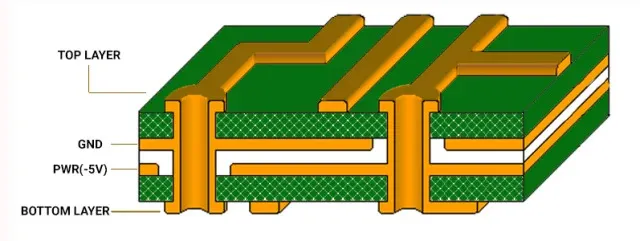
1. Layer Stack-Up Configuration
The arrangement of layers in a 4-layer PCB significantly impacts performance and manufacturability. A common stack-up is:
- Top Layer: Signal routing and component placement
- Inner Layer 1: Ground plane for EMI shielding
- Inner Layer 2: Power plane for stable voltage distribution
- Bottom Layer: Additional signal routing or ground
This configuration minimizes noise and ensures stable power delivery, which is vital for high-speed designs operating at frequencies above 100 MHz. However, confirm with your manufacturing partner that the stack-up aligns with their capabilities, as deviations can lead to impedance mismatches (e.g., a target of 50 ohms for controlled impedance lines might vary by ±10% if not properly managed).
Tip: Keep the ground and power planes as uninterrupted as possible to reduce EMI. Avoid splitting planes unless absolutely necessary for specific circuit requirements.
2. Component Placement and Routing
Efficient component placement reduces routing complexity and manufacturing errors. Place high-speed components close to their connectors to minimize signal delay, and group related components to shorten trace lengths. For example, in a design with a microcontroller operating at 48 MHz, placing decoupling capacitors within 0.1 inches of power pins can prevent voltage drops and noise issues.
For routing, prioritize critical signals on the top and bottom layers, using inner layers for power and ground. Maintain a minimum trace width and spacing (often 6 mils for standard processes) to avoid manufacturing defects like shorts or opens during etching.
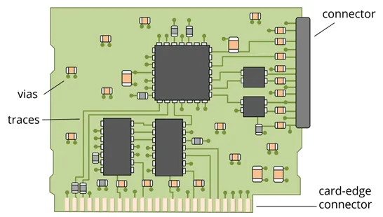
3. Via Design and Placement
Vias connect different layers in a 4-layer PCB, but excessive or poorly placed vias can complicate manufacturing and increase costs. Use through-hole vias for simplicity in mass production, as they are easier to fabricate than blind or buried vias. Keep via diameters at least 0.3 mm and ensure an annular ring of 0.15 mm to prevent drilling issues.
Minimize the number of vias by optimizing routing, as each via adds a potential point of failure during assembly. Also, avoid placing vias under components, as this can interfere with soldering processes like reflow.
Strategies for 4-Layer PCB Cost Reduction
Cost is a critical factor in 4-layer PCB mass production. While 4-layer boards are more expensive than 2-layer ones, there are several ways to keep expenses in check without compromising quality.
1. Standardize Materials and Specifications
Using standard materials like FR-4 with a dielectric constant of 4.2-4.5 can significantly lower costs compared to specialized laminates. Stick to common board thicknesses (e.g., 1.6 mm) and copper weights (1 oz or 2 oz per square foot) that are widely available and supported by most manufacturers. Non-standard specifications often lead to higher tooling costs or longer lead times.
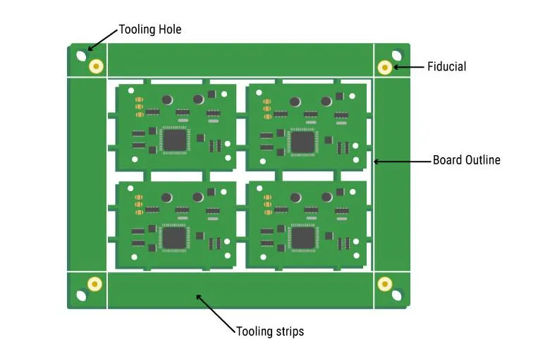
2. Optimize Panel Utilization
During mass production, PCBs are fabricated in panels. Designing your board to fit efficiently within a standard panel size (e.g., 18 x 24 inches) reduces material waste and lowers costs. Avoid odd shapes or oversized boards that require custom panelization, as this increases production expenses.
For example, if your PCB dimensions are 2 x 3 inches, arranging multiple units in a grid pattern on the panel can maximize yield, potentially fitting 50 or more boards per panel, depending on spacing and border requirements.
3. Minimize Layer Transitions
Reducing the number of layer transitions through vias not only improves signal integrity but also cuts manufacturing costs. Each via requires drilling and plating, adding to the expense. Plan your routing to keep signals on the same layer whenever possible.
Ensuring 4-Layer PCB Quality Control in Mass Production
Quality control is non-negotiable in 4-layer PCB manufacturing. Defects in a single board can lead to costly rework or product failures. Here’s how to maintain high standards during mass production.
1. Design Rule Checks (DRC)
Before sending your design to production, run a thorough DRC to catch potential issues like trace spacing violations or unconnected nets. Most design software flags errors such as traces closer than 6 mils or vias with insufficient annular rings, preventing manufacturing defects.
2. Electrical Testing
Specify electrical testing, such as flying probe or bed-of-nails testing, to verify connectivity and detect shorts or opens. For high-speed designs, request impedance testing to ensure traces meet specifications (e.g., 50 ohms ±10% for controlled impedance lines). While testing adds to the upfront cost, it prevents expensive failures in the field.
3. Visual and Automated Inspection
Manufacturers often perform Automated Optical Inspection (AOI) to check for soldering defects, misaligned components, or surface issues. Request detailed inspection reports to ensure every batch meets quality standards. For critical applications, consider X-ray inspection to verify internal layer alignment and via integrity.
Manufacturing Challenges and How to Avoid Them
Even with a well-designed 4-layer PCB, manufacturing challenges can arise during mass production. Here are common issues and solutions:
1. Layer Misalignment
Misalignment between layers can cause signal integrity problems or connection failures. To avoid this, ensure your design files include clear layer registration marks, and work with a manufacturer that uses advanced alignment equipment. Typical alignment tolerance should be within ±0.1 mm for a standard 4-layer board.
2. Thermal Stress During Assembly
During soldering, thermal stress can cause delamination or warping, especially if the board material isn’t suited for high-temperature processes like reflow soldering at 260°C. Specify materials with a high glass transition temperature (Tg), such as FR-4 with a Tg of 150°C or higher, to withstand assembly conditions.
3. Supply Chain Delays
Material shortages or long lead times for non-standard components can delay production. To mitigate this, use widely available components and materials, and maintain open communication with your manufacturing partner to anticipate potential bottlenecks.

Scaling Up: Tips for Successful 4-Layer PCB Mass Production
Once your design is ready and initial prototypes are validated, scaling to mass production requires a few additional steps:
- Prototype Validation: Test a small batch of boards to confirm performance under real-world conditions. For example, if your design operates at 5V with a current draw of 500 mA, verify that power distribution remains stable across all units.
- Documentation: Provide detailed assembly drawings, Bill of Materials (BOM), and Gerber files to avoid miscommunication with the manufacturer.
- Volume Pricing: Negotiate pricing for larger quantities. Costs per unit often drop significantly at volumes above 1,000 units due to economies of scale.
Conclusion
Optimizing 4-layer PCB designs for mass production requires careful attention to design, cost, and quality. By focusing on a manufacturable stack-up, efficient component placement, and robust 4-layer PCB quality control, you can ensure a smooth transition from prototype to large-scale production. Implementing 4-layer PCB cost reduction strategies, such as standardizing materials and optimizing panel usage, further enhances profitability without compromising performance.
Whether you're developing consumer electronics or industrial equipment, these 4-layer PCB manufacturing practices can help you achieve reliable, high-quality results. Start with a solid 4-layer PCB design for manufacturing, collaborate closely with your production partner, and prioritize testing to deliver products that meet or exceed expectations.


