 ALLPCB


Are you struggling to maintain signal integrity in your high-speed PCB designs? The secret often lies in mastering PCB stackup design for impedance control. A well-planned stackup ensures that your signals travel without distortion, reducing noise and improving performance. In this comprehensive guide, we’ll dive into the essentials of PCB stackup design, focusing on impedance calculation, layer selection, and material choices to help you achieve optimal results for your projects.
What Is PCB Stackup Design and Why Does It Matter for Impedance Control?
PCB stackup design refers to the arrangement of conductive copper layers and insulating dielectric materials in a printed circuit board. It’s like building a multi-story structure where each floor (layer) has a specific purpose—some carry signals, others provide power or ground. The way these layers are stacked directly impacts how signals behave, especially in high-speed designs where impedance control is critical.
Impedance control ensures that the electrical signals traveling through your PCB maintain a consistent resistance to changes in current. Without it, you risk signal reflections, crosstalk, and data loss, which can ruin the performance of devices like high-speed processors or communication systems. A proper stackup design aligns the layers and materials to match the desired impedance, often targeting values like 50 ohms for single-ended traces or 100 ohms for differential pairs.
Let’s explore how to design a stackup that keeps impedance in check, using practical steps and real-world considerations.
Understanding Impedance in PCB Design
Impedance in a PCB is the opposition to alternating current caused by the combination of resistance, inductance, and capacitance in a trace. For high-speed signals, controlling impedance is crucial because mismatches can cause signal reflections. Imagine sending a signal down a trace with an impedance of 50 ohms, but it hits a section with 75 ohms—part of the signal bounces back, creating noise and degrading performance.
The goal of impedance control is to maintain a consistent value along the signal path. This is where PCB stackup design comes in. The stackup determines the spacing between traces and reference planes (like ground or power layers), as well as the dielectric properties of the materials used. Both factors heavily influence impedance.
Key Factors in PCB Stackup Impedance Calculation
Calculating impedance for your PCB stackup involves several variables. Here’s a breakdown of the main factors you need to consider:
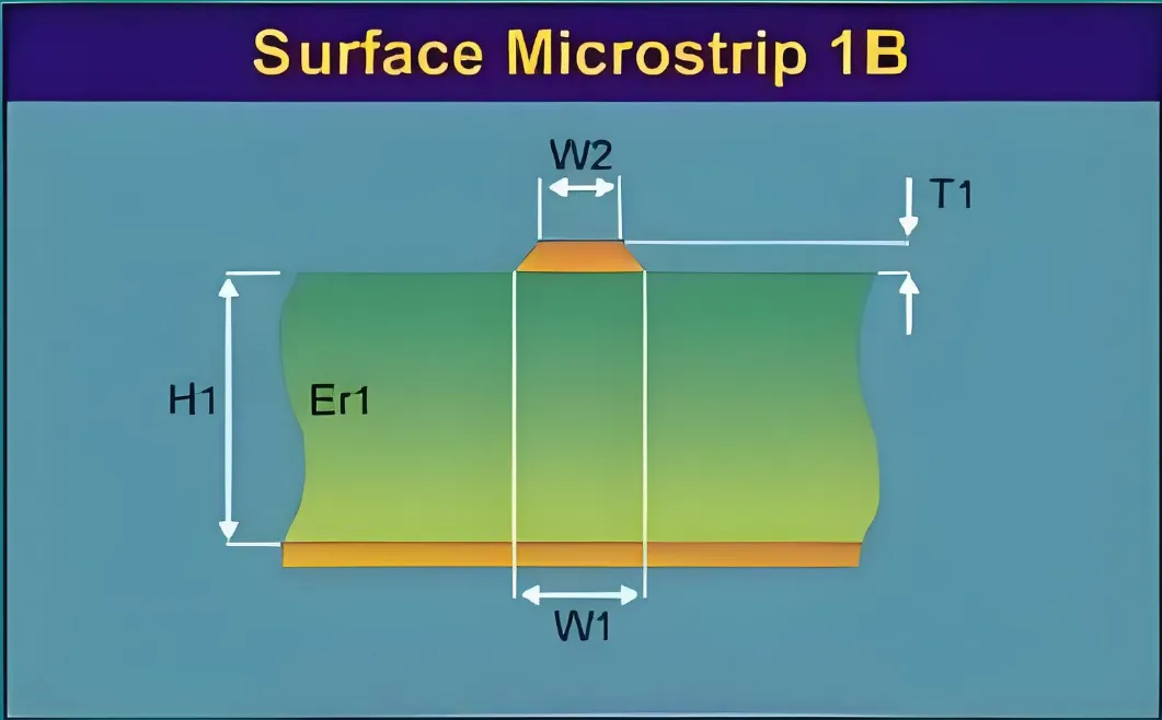
1. Trace Width and Thickness
The width and thickness of your copper traces directly affect impedance. Wider traces generally have lower impedance, while narrower traces increase it. For example, a 5-mil wide trace on a 1-ounce copper layer might achieve a 50-ohm impedance when paired with a specific dielectric thickness, but narrowing it to 3 mils could push the impedance higher.
2. Dielectric Thickness and Constant (Dk)
The dielectric material between layers acts as an insulator and impacts how fast signals travel. The dielectric constant (Dk) measures how much a material slows down an electric field compared to a vacuum. Common materials like FR-4 have a Dk of around 4.2 to 4.5, while high-speed designs might use materials with a Dk of 3.0 or lower to reduce signal delay. Thinner dielectric layers bring traces closer to reference planes, lowering impedance.
3. Reference Plane Proximity
Signal layers need a nearby reference plane (ground or power) to maintain consistent impedance. The closer the plane, the lower the impedance due to increased capacitance. For instance, a signal layer separated from a ground plane by 5 mils of dielectric might target 50 ohms, but increasing that distance to 10 mils could raise the impedance significantly.
Using online impedance calculators or PCB design software can simplify these calculations. Many tools allow you to input trace dimensions, dielectric properties, and layer spacing to predict impedance values before manufacturing.
Choosing Layer Stackup for Impedance Control
Selecting the right layer stackup is a balancing act between signal integrity, manufacturing cost, and board complexity. Here are key considerations when designing your stackup for impedance control:
1. Number of Layers
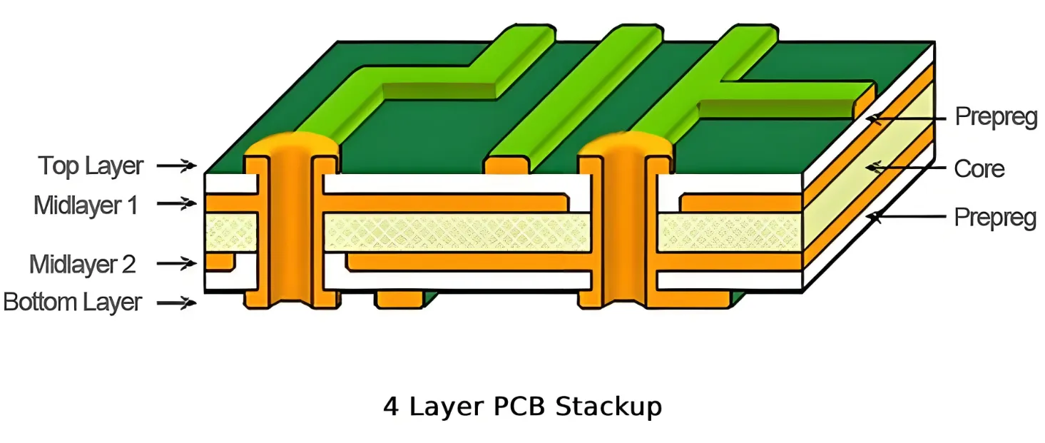
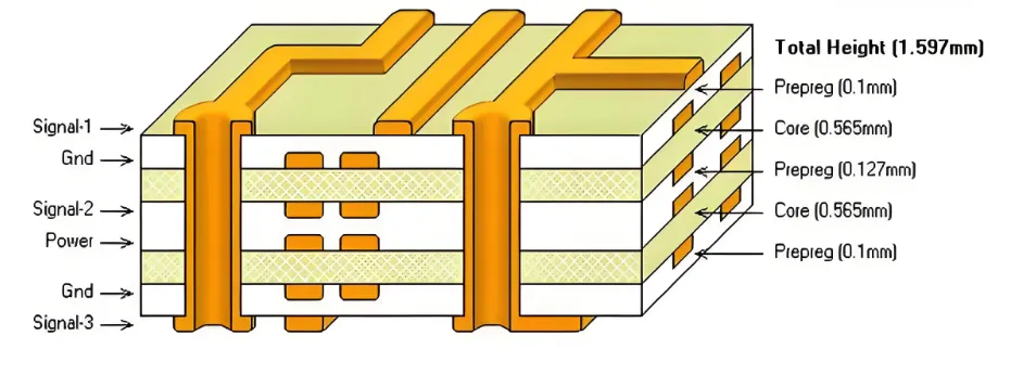
Simple designs might use a 2-layer board, with signals on one side and ground on the other. However, for high-speed applications, 4, 6, or even 10-layer boards are common. More layers allow dedicated ground and power planes, which act as reference planes for signal layers, improving impedance stability. For example, a 6-layer stackup might include two signal layers on the outside, two inner signal layers, and dedicated power and ground planes in the middle.
2. Symmetry in Stackup
A symmetrical stackup prevents warping during manufacturing and ensures consistent electrical performance. If you have signal layers on the top and bottom, balance the dielectric thickness and copper distribution across the board. An unbalanced stackup can lead to uneven impedance values across layers.
3. Signal Layer Placement
Place high-speed signal layers next to a reference plane to control impedance tightly. Outer layers are often less ideal for controlled impedance traces because they’re farther from planes and more exposed to external noise. Inner layers, buried between planes, offer better precision—tolerances can be as tight as ±5% compared to ±10% or more on outer layers.
4. Power and Ground Plane Placement
Position power and ground planes close together to create a natural decoupling capacitor effect, reducing noise in high-speed designs. For instance, in a 10-layer board, placing ground and power planes in the center with minimal dielectric spacing (e.g., 3-5 mils) can enhance this effect.
PCB Material Selection for Impedance
The materials you choose for your PCB play a huge role in impedance control. Let’s look at the key aspects of material selection:
1. Dielectric Material
Standard FR-4 is the go-to material for many designs due to its cost-effectiveness and Dk of around 4.2-4.5. However, for high-frequency signals (above 1 GHz), FR-4 can introduce signal loss due to its higher dissipation factor (Df). Materials like Rogers 4350B, with a Dk of 3.48 and lower Df, are better suited for high-speed applications, though they cost more.
2. Dielectric Thickness
Thinner dielectrics reduce the distance between traces and reference planes, lowering impedance and allowing for finer trace widths. However, very thin layers can increase manufacturing costs and risk signal crosstalk if not spaced properly. A common range for dielectric thickness in impedance-controlled designs is 3 to 10 mils, depending on the target impedance.
3. Copper Thickness
Copper thickness affects trace resistance and heat dissipation. Standard boards use 1-ounce copper (1.4 mils thick), but high-current or high-speed designs might require 2-ounce copper (2.8 mils) for better performance. Thicker copper lowers impedance slightly, so it’s a factor in calculations.
Work closely with your PCB manufacturer to select materials that match your impedance requirements and budget. Many manufacturers provide material libraries or stackup recommendations based on your design goals.
Practical Tips for Designing a Stackup with Impedance in Mind
Now that we’ve covered the basics, here are actionable tips to guide your PCB stackup design process:
- Start with Simulation Tools: Use software with built-in impedance calculators to model your stackup before fabrication. Input your trace dimensions, layer spacing, and material properties to predict results.
- Consult Manufacturer Guidelines: Your PCB fabricator can provide stackup templates and material options tailored for impedance control. They often specify achievable tolerances, like ±10% for standard processes or ±5% for advanced builds.
- Test and Validate: After manufacturing, use a Time Domain Reflectometer (TDR) to measure actual impedance and compare it to your target. This helps catch discrepancies early.
- Minimize Via Impact: Vias can introduce impedance mismatches. Keep them short and use back-drilling for high-speed designs to remove unused via stubs.
- Account for Frequency: Higher frequencies demand tighter impedance control. For signals above 5 GHz, consider advanced materials and thinner dielectrics to maintain signal integrity.
Common Challenges in PCB Stackup Design for Impedance Control
Even with careful planning, challenges can arise. Here are a few common issues and how to address them:
1. Manufacturing Tolerances
Variations in dielectric thickness or trace etching can shift impedance values. Standard manufacturing might achieve ±10% tolerance, but for critical designs, opt for tighter controls (e.g., ±5%) at an added cost.
2. Signal Loss at High Frequencies
At frequencies above 1 GHz, dielectric loss and skin effect in copper traces degrade signals. Choose low-loss materials and keep traces short to minimize this.
3. Cost Constraints
High-performance materials and complex stackups increase costs. Balance performance needs with budget by prioritizing critical layers for advanced materials while using standard options elsewhere.
Conclusion: Mastering PCB Stackup for Optimal Impedance Control
Designing a PCB stackup for impedance control is a critical step in ensuring signal integrity, especially for high-speed and high-frequency applications. By carefully calculating impedance, choosing the right layer stackup, and selecting appropriate materials, you can avoid common pitfalls like signal reflections and crosstalk. Remember to leverage simulation tools, collaborate with your manufacturer, and validate your design to achieve the best results.
Whether you’re working on a simple 2-layer board or a complex 10-layer design, the principles of PCB stackup design remain the same—plan meticulously, prioritize reference planes, and match materials to your performance needs. With these strategies, you’ll be well-equipped to tackle impedance control and deliver reliable, high-performing PCBs for any project.


