 ALLPCB


Flexible printed circuit boards (FPCBs) are transforming electronics design, enabling compact, lightweight, and durable solutions for industries like consumer electronics, medical devices, automotive, and aerospace. Their ability to bend, fold, and twist makes them ideal for applications where rigid PCBs fall short. However, designing flexible PCBs requires careful consideration of materials, layout, and manufacturing processes to ensure reliability and performance. In this blog, we share best practices for designing bendable circuits, drawing from industry insights to help engineers create robust and efficient FPCBs.
Whether you're designing a wearable device or a complex automotive system, these guidelines will help you optimize your flexible PCB for durability, functionality, and manufacturability.
Understanding Flexible PCBs: Key Characteristics
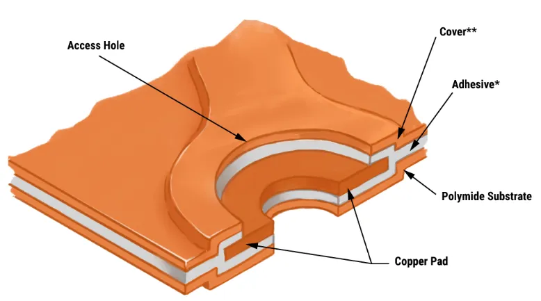
Flexible PCBs differ from rigid PCBs in their construction and behavior. They consist of a thin, flexible substrate - typically polyimide (PI) or polyester - layered with conductive copper traces and a protective coverlay. This structure allows FPCBs to conform to unique shapes, withstand vibrations, and fit into tight spaces. According to industry standards like IPC-6013, flexible PCBs can be single-sided, double-sided, or multilayer, with rigid-flex variants combining flexible and rigid sections.
Key characteristics include:
-
Flexibility: FPCBs can bend up to 360 degrees, with some designs rated for over 500 million flex cycles.
-
Lightweight: They occupy about 10% of the space and weight of rigid PCBs, ideal for compact devices.
-
Thermal Stability: Polyimide substrates resist temperatures from -200°C to 400°C, suitable for harsh environments.
-
Reliability: Fewer interconnects reduce solder joints and failure points, enhancing durability.
Best Practices for Flexible PCB Design
To achieve a reliable and manufacturable flexible PCB, engineers must address material selection, bend radius, trace routing, and other critical factors. Below, we outline actionable best practices.
1. Select the Right Materials
Material choice is the foundation of a successful FPCB design. The substrate, copper type, and adhesives must balance flexibility, durability, and electrical performance.
-
Substrate: Polyimide (PI) is the most common substrate due to its high thermal resistance (up to 400°C) and tensile strength. For cost-sensitive applications, polyester (PET) is an alternative but offers lower heat resistance. Use adhesive-less laminates for thinner designs to reduce moisture absorption and cracking risks.
-
Copper Type: Rolled Annealed (RA) copper is preferred for dynamic flexing applications because its elongated grain structure enhances ductility. Electro-Deposited (ED) copper is less flexible and better suited for static bends. For example, RA copper can withstand 10,000+ flex cycles compared to ED copper's 1,000 cycles in dynamic applications.
-
Adhesives: Acrylic adhesives are flexible but may crack under repeated bending. Epoxy or pressure-sensitive adhesives (PSAs) offer better durability for rigid-flex transitions. Avoid thick adhesive layers, as they increase stress and reduce flexibility.

2. Optimize Bend Radius for Reliability
The bend radius - the minimum curvature a flex area can withstand without damaging traces - is critical for FPCB longevity. A tighter bend radius increases stress on copper traces, risking fatigue fractures.
-
Calculate Bend Radius: According to IPC-2223, the minimum bend radius depends on the number of layers:
-
Single-layer: 6x the flex thickness (e.g., 0.1 mm thickness = 0.6 mm radius).
-
Double-layer: 12x the flex thickness.
-
Multilayer: 24x the flex thickness.
-
-
Avoid Sharp Bends: Use gradual curves instead of 90-degree bends to minimize strain. For example, a 45-degree curve reduces stress by up to 30% compared to a sharp bend.
-
Dynamic vs. Static Bends: For dynamic applications (e.g., wearables), maintain a larger bend radius (10x thickness) to ensure 500,000+ flex cycles. Static bends (e.g., folded during assembly) can use tighter radii (6x thickness).
3. Design Traces for Flexibility and Signal Integrity
Trace routing in flexible PCBs must account for mechanical stress and electrical performance, especially in high-frequency applications.
-
Use Hatched Polygons: Solid copper planes reduce flexibility and create stress points. Hatched polygons, especially hexagonal patterns, distribute stress evenly across 0°, 60°, and 120° angles, improving flexibility by up to 50%. A typical hatch pattern uses 0.015" wide traces with 0.025" spacing.
-
Stagger Traces: In multilayer designs, stagger traces across layers to avoid overlapping, which reduces stress concentration. Maintain a 10-mil clearance between traces in bend areas.
-
Control Impedance: For high-speed signals (e.g., 5 Gbps USB 3.0), use cross-hatched ground planes to maintain impedance (typically 50Ω or 100Ω). A cross-hatch with a 0.293 conductor-to-pitch ratio removes 50% of copper, increasing flexibility without compromising signal integrity.
-
Avoid Vias in Bend Areas: Vias are prone to cracking under flexing. If unavoidable, place vias at least 20 mils from bend areas and use teardrop annular rings for traces thinner than 20 mils to enhance structural integrity.

4. Incorporate Stiffeners for Mechanical Support
PCB stiffener adds rigidity to specific FPCB areas, such as connector regions or component mounting zones, to prevent bending-related damage.
-
Material Choices: Polyimide or FR4 stiffeners are common, with thicknesses of 0.1-0.5 mm for polyimide and 0.8-1.6 mm for FR4. Aluminum or stainless steel stiffeners are used for high-stress applications, such as automotive modules.
-
Placement: Place stiffeners at least 50 mils from vias to avoid cracking. For example, in a smartphone FPCB, stiffeners reinforce the connector area while allowing the rest of the circuit to flex.
-
Attachment: Use thermally cured acrylic adhesives for permanent bonding or PSAs for reworkable designs. Ensure adhesive thickness does not exceed 10% of the overall construction to maintain flexibility.
5. Collaborate with Fabricators Early
Close collaboration with your PCB manufacturer ensures your design aligns with fabrication capabilities, reducing costs and delays.
-
Stackup Design: Share your stackup early to confirm material availability and layer alignment. Misregistration between layers should not exceed ±0.005".
-
Fabrication Feedback: Fabricators can advise on bend requirements, keepout regions, and stiffener placement. For instance, automated fluid dispensing for stiffener adhesives can reduce costs by 20% compared to manual application.
-
Documentation: Provide clear Gerber files and a detailed fabrication drawing, specifying bend radius, impedance values (e.g., 50Ω ±10%), and surface finish (e.g., ENIG for solderability).
6. Test for Reliability and Compliance
Testing ensures your FPCB meets performance and durability standards, especially for demanding applications like medical implants or aerospace systems.
-
IPC Standards: Adhere to IPC-6013 for flex PCB quality and IPC-2223 for design guidelines. Test for warpage (≤0.75%) and impedance tolerance (±10%).
-
Flex Cycle Testing: For dynamic applications, simulate 500,000+ flex cycles to verify copper fatigue resistance. Use RA copper to achieve a fatigue life of 10,000 cycles in tight radii (0.6 mm).
-
Environmental Testing: Test for thermal stability (-200°C to 400°C) and chemical resistance, especially for oil and gas applications.
Applications of Flexible PCBs
Flexible PCBs shine in applications requiring compact, durable, and dynamic designs. Examples include:
-
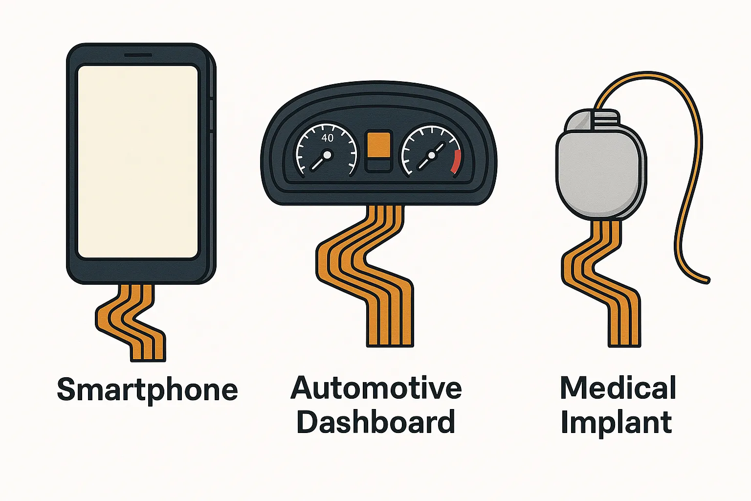
Consumer Electronics: Smartphones and wearables use FPCBs to fit circuitry into slim profiles, with 0.1 mm thick substrates enabling tight folds.
Read more: Flexible PCBs for Foldable Phones: Design and Manufacturing Innovations
-
Automotive: Dashboard displays and lighting systems use rigid-flex PCBs to withstand vibrations, with stiffeners ensuring connector reliability.
Read more: Bending the Rules: How Flexible PCBs are Revolutionizing Automotive Electronics Manufacturing
-
Medical Devices: Implantable devices leverage biocompatible polyimide FPCBs, with 0.05 mm substrates for flexibility inside the body.
Read more: Flexible PCB Design for Medical Wearables: Balancing Performance and Biocompatibility
-
Aerospace: Satellites use lightweight FPCBs (0.07 mm copper strips) to reduce payload weight, with thermal vias for heat dissipation.
How ALLPCB Supports Flexible PCB Design
At ALLPCB, we empower engineers to bring their flexible PCB designs to life with our advanced manufacturing capabilities and global logistics. Our quick-turn prototyping service delivers FPCB prototypes in as little as 24 hours, allowing you to test and iterate designs rapidly. With expertise in polyimide substrates, RA copper, and precise impedance control, we ensure your FPCBs meet IPC standards for reliability and performance. Our global supply chain and automated production lines streamline fabrication, reducing costs and lead times for projects ranging from wearables to aerospace systems.
Conclusion: Designing Flexible PCBs with Confidence
Flexible PCB design demands a balance of material selection, mechanical considerations, and electrical performance. By following best practices - choosing the right materials, optimizing bend radius, designing flexible traces, incorporating stiffeners, collaborating with fabricators, and rigorous testing - you can create FPCBs that are durable, efficient, and manufacturable. Whether you're working on a compact wearable or a rugged automotive system, these guidelines will help you achieve success.
Ready to start your flexible PCB project? Apply these best practices and partner with a trusted manufacturer to turn your vision into reality. Let's bend the future of electronics together.


