Designing a wearable blood pressure monitor PCB is a complex yet rewarding task for engineers and hobbyists looking to innovate in the medical device space. Whether you're working on a DIY PCB project or developing a commercial medical device PCB, you’ll face unique challenges like sensor integration, power management, and ensuring accuracy in a compact form factor. In this blog, we’ll explore these PCB design challenges in detail and provide practical solutions to help you create a reliable and efficient wearable blood pressure monitor.
At ALLPCB, we understand the intricacies of crafting PCBs for specialized applications like medical devices. This guide will walk you through the key hurdles in designing a blood pressure monitor PCB and offer actionable tips to overcome them, ensuring your project meets both performance and regulatory standards.
Why Wearable Blood Pressure Monitors Matter
Wearable blood pressure monitors are transforming healthcare by enabling continuous, non-invasive monitoring of vital signs. Unlike traditional cuff-based devices, wearables offer convenience and real-time data, making them ideal for patients with hypertension or those monitoring cardiovascular health. However, designing the PCB for such a device requires precision, as it must integrate sensors, manage power efficiently, and fit into a small, user-friendly design.
The demand for these devices is growing, with the global wearable medical device market expected to reach significant milestones in the coming years. For engineers and DIY enthusiasts, this presents an opportunity to create innovative solutions, provided the PCB design challenges are addressed effectively.
Key Components of a Blood Pressure Monitor PCB
Before diving into the challenges, let’s break down the essential components of a wearable blood pressure monitor PCB. Understanding these elements is crucial for tackling sensor integration and other design hurdles.
- Sensors: Optical sensors (like photoplethysmography or PPG) or pressure sensors are used to detect blood flow or pressure changes. These often require precise placement and noise reduction for accurate readings.
- Microcontroller Unit (MCU): The MCU processes sensor data, performs calculations, and controls the device. Low-power MCUs are preferred for wearables to extend battery life.
- Power Management Circuitry: This includes batteries, voltage regulators, and energy-efficient designs to ensure long-term operation in a compact device.
- Communication Module: Bluetooth or other wireless technologies transmit data to a smartphone or cloud platform for analysis.
- Display or Interface: A small OLED screen or LED indicators provide real-time feedback to the user.
Each of these components must work seamlessly together, which brings us to the core challenges in PCB design for such devices.
PCB Design Challenges for Wearable Blood Pressure Monitors
Creating a PCB for a wearable blood pressure monitor involves overcoming several technical obstacles. Below, we detail the most common challenges faced during the design process.
1. Sensor Integration and Signal Accuracy
One of the biggest hurdles in designing a medical device PCB is integrating sensors that deliver accurate and consistent readings. Wearable blood pressure monitors often rely on optical sensors to measure pulse wave velocity or pressure changes. However, factors like skin tone, motion artifacts, and ambient light can interfere with sensor performance, leading to inaccurate data.
Additionally, the analog signals from these sensors are typically weak, with amplitudes in the millivolt range (e.g., 1-10 mV for PPG signals). Amplifying these signals without introducing noise is a significant challenge, as electrical interference can distort readings.
2. Miniaturization and Space Constraints
Wearable devices must be small and lightweight to ensure user comfort. This means the PCB layout must fit into a constrained space, often no larger than a few square centimeters. Balancing the need for multiple components (sensors, MCU, battery) while maintaining a compact design is a constant struggle. Overcrowding can also lead to heat dissipation issues, which can affect sensor accuracy and user safety.
3. Power Management and Battery Life
Power efficiency is critical for wearables, as users expect devices to last for days or even weeks on a single charge. Designing a PCB with low-power components and efficient circuitry is essential. For example, the MCU might consume only 50-100 μA in sleep mode, but improper design could lead to unnecessary power drain, shortening battery life.
Moreover, the charging circuit must be integrated into the PCB without adding bulk, and overvoltage protection is necessary to prevent damage to sensitive medical components.
4. Regulatory and Safety Standards
Medical devices, even DIY projects, must adhere to strict regulatory standards like ISO 13485 for quality management and IEC 60601 for electrical safety. Ensuring that the PCB design meets these standards adds complexity, as it requires rigorous testing for electromagnetic compatibility (EMC) and biocompatibility of materials used in the device.
Failure to comply with these standards can result in legal issues or, worse, harm to users due to inaccurate readings or electrical hazards.
5. Data Processing and Connectivity
A wearable blood pressure monitor must process data in real-time and often transmit it to external devices via Bluetooth or other wireless protocols. This requires a robust communication module on the PCB, which can introduce noise if not properly shielded. Additionally, the MCU must handle complex algorithms to calculate systolic and diastolic pressure from raw sensor data, often requiring high computational power in a low-power design.

Solutions to Overcome PCB Design Challenges
While the challenges of designing a blood pressure monitor PCB are significant, they are not insurmountable. Below are practical solutions to address each issue, ensuring your DIY PCB or medical device PCB performs reliably.
1. Optimizing Sensor Integration for Accuracy
To improve sensor accuracy, start by selecting high-quality sensors with built-in noise reduction features. For optical sensors, use shielding to minimize interference from ambient light. Implement analog front-end (AFE) circuits to amplify weak signals (e.g., using an operational amplifier with a gain of 100) while filtering out noise with low-pass filters (cut-off frequency around 10 Hz for PPG signals).
Additionally, place sensors close to the skin contact point on the wearable device and use flexible PCB materials if needed to conform to the body’s shape. Software algorithms can also help by compensating for motion artifacts through adaptive filtering techniques.
2. Addressing Miniaturization with Smart Layouts
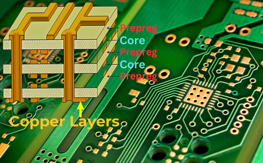
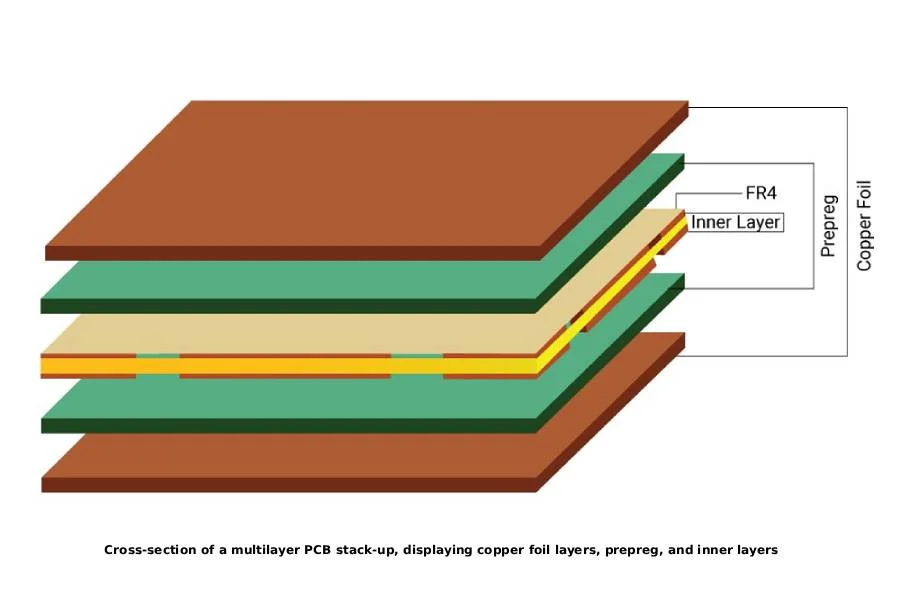
To tackle space constraints, use multi-layer PCBs to stack components vertically, reducing the overall footprint. Surface-mount technology (SMT) components are ideal for wearables due to their small size. Tools for PCB design can help optimize trace routing to avoid overcrowding, ensuring that signal integrity is maintained with minimal crosstalk.
For heat dissipation, incorporate thermal vias and copper pours in the PCB layout to distribute heat evenly. If space allows, add small heat sinks or use materials with high thermal conductivity.
3. Enhancing Power Management
Choose low-power components, such as MCUs with sleep modes that reduce current draw to below 100 μA when idle. Implement power gating to shut off unused circuits during operation. For battery life, select lithium-ion or lithium-polymer batteries with capacities around 100-200 mAh for compact wearables, and integrate efficient DC-DC converters to maintain stable voltage levels (e.g., 3.3V for most MCUs).
Design the charging circuit with overvoltage and overcurrent protection using ICs that limit input to safe levels (e.g., 4.2V for lithium batteries). This ensures safety and extends the lifespan of the device.
4. Meeting Regulatory Standards
To comply with medical device standards, start by designing the PCB with safety in mind. Use biocompatible materials for parts that contact the skin and ensure proper insulation to prevent electrical shocks. Conduct EMC testing early in the design phase to identify and mitigate interference issues, such as using ground planes to reduce noise.
Partner with certification bodies to validate your design against standards like IEC 60601. For DIY PCB projects, while full certification may not be required, following these guidelines ensures a safer and more reliable device.
5. Streamlining Data Processing and Connectivity
For real-time data processing, select an MCU with sufficient processing power (e.g., 32-bit ARM Cortex-M processors) to handle complex algorithms without draining power. Use dedicated hardware accelerators if available to offload tasks like signal filtering.
For connectivity, integrate Bluetooth Low Energy (BLE) modules, which consume less power (around 10 mA during transmission) compared to standard Bluetooth. Shield the communication module with proper grounding to prevent interference with sensor signals. Test the wireless range (typically 10-15 meters for BLE) to ensure reliable data transmission.

Tips for DIY PCB Designers Building Blood Pressure Monitors
If you’re a hobbyist or engineer working on a DIY PCB for a blood pressure monitor, keep these additional tips in mind to simplify the process and improve outcomes.
- Start Small: Begin with a prototype using breakout boards for sensors and MCUs before designing a custom PCB. This allows you to test functionality without committing to a full layout.
- Use Open-Source Resources: Leverage open-source libraries for signal processing algorithms to save time on coding complex calculations like blood pressure estimation.
- Iterate and Test: Build multiple versions of your PCB, testing each for signal accuracy and power consumption. Use oscilloscopes to measure signal noise levels (aim for less than 1 mV of ripple in amplified signals).
- Document Everything: Keep detailed notes on your design choices and test results. This is especially useful for troubleshooting issues like unexpected power drain or sensor drift.
The Future of Wearable Blood Pressure Monitor PCB Design
The field of wearable medical devices is evolving rapidly, with advancements in sensor technology and AI-driven data analysis. Future blood pressure monitor PCBs may incorporate machine learning algorithms directly on the device to predict health trends based on continuous data. Additionally, innovations in flexible and stretchable PCBs could make wearables even more comfortable and seamless to use.
As an engineer or DIY enthusiast, staying updated on these trends can give you a competitive edge in designing cutting-edge medical device PCBs. Collaborating with platforms that provide high-quality PCB manufacturing services can also streamline your development process, ensuring precision and reliability in every prototype.
Conclusion
Designing a wearable blood pressure monitor PCB comes with its fair share of challenges, from sensor integration to power management and regulatory compliance. However, with the right approach—optimizing layouts, selecting low-power components, and adhering to safety standards—you can create a device that is both functional and user-friendly. Whether you’re tackling a DIY PCB project or developing a commercial medical device PCB, the solutions outlined in this guide provide a roadmap to success.
 ALLPCB


