 ALLPCB


Automated Optical Inspection (AOI) systems play a vital role in ensuring the quality of IPC Class 2 assembly for printed circuit boards (PCBs). If you're looking to understand how AOI systems enhance defect detection, minimize false calls, and optimize programming strategies and inspection parameters, you're in the right place. In this detailed guide, we'll explore how AOI technology supports IPC Class 2 standards, offering practical insights into achieving high-quality PCB assembly.
What is IPC Class 2 Assembly and Why Does AOI Matter?
IPC Class 2 assembly refers to a category of PCB manufacturing defined by the Institute of Printed Circuits (IPC) standards, specifically targeting dedicated service electronic products. These products, often found in industrial and commercial applications, require high reliability and extended performance but do not demand the stringent criteria of Class 3 (used in aerospace or medical devices). Think of Class 2 as the sweet spot for many everyday electronics where quality and cost must balance effectively.
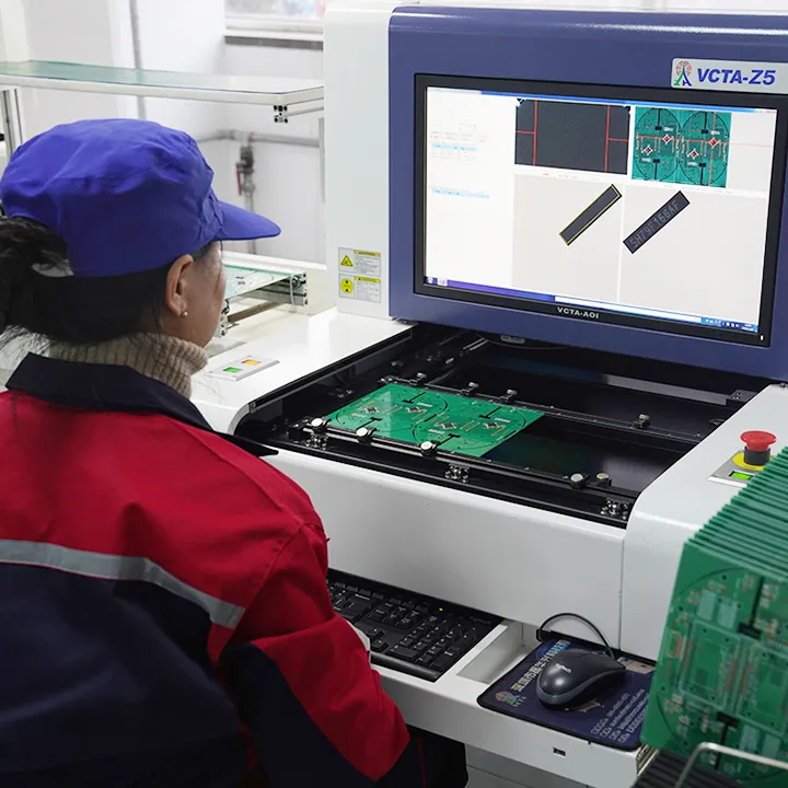
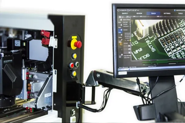
AOI systems are critical in this context because they provide a non-contact, automated method to inspect PCBs for defects during assembly. By using high-resolution cameras, advanced lighting, and sophisticated algorithms, AOI identifies issues like missing components, misalignments, solder defects, and more. For Class 2 assembly, where consistent quality is essential, AOI ensures that defects are caught early, reducing rework costs and improving overall efficiency.
Understanding the Role of AOI Systems in Defect Detection
Defect detection is at the heart of any AOI system. During IPC Class 2 assembly, PCBs go through multiple stages—solder paste application, component placement, and reflow soldering—each presenting opportunities for errors. AOI systems step in to catch these issues before they escalate into costly failures.
Common defects detected by AOI include:
- Missing Components: Ensuring every part is placed as per the design.
- Misaligned Components: Detecting parts that are not correctly positioned, which could lead to connectivity issues.
- Solder Joint Defects: Identifying insufficient solder, bridging, or cold joints that affect electrical performance.
- Billboard or Tombstone Effects: Spotting components that stand upright or lift off the board during soldering.
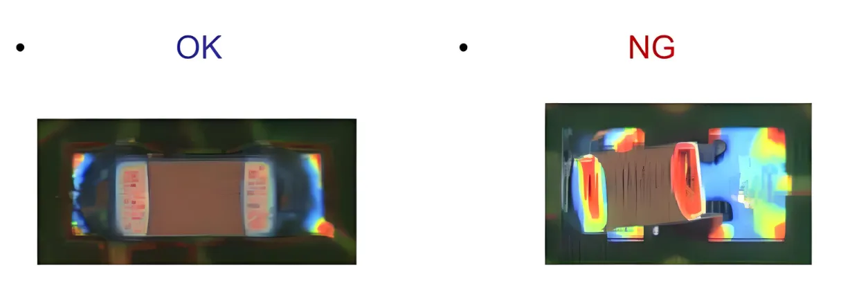
AOI systems use high-resolution imaging to capture detailed visuals of the PCB surface, comparing them against a predefined "golden board" or CAD data. For instance, modern systems can detect defects as small as 0.01 mm, ensuring even minute deviations are flagged. This precision is crucial for Class 2 assemblies, where reliability is non-negotiable for end users.
Minimizing False Calls in AOI Systems
While AOI systems are powerful, they are not immune to errors, particularly false calls—situations where the system flags a non-defect as a problem. False calls can slow down production, increase manual verification time, and lead to unnecessary rework. For IPC Class 2 assembly, where efficiency matters, reducing false calls is a priority.
Several factors contribute to false calls in AOI systems:
- Lighting Variations: Inconsistent lighting can cause shadows or reflections that mimic defects.
- Board Warpage: Slight bending of the PCB can distort images, leading to incorrect analysis.
- Component Variations: Minor differences in component appearance (e.g., color or markings) can confuse the system.
To address this, manufacturers can take steps like calibrating lighting to ensure uniform illumination, using 3D AOI systems to account for board warpage, and updating the reference database to accommodate component variations. By fine-tuning these elements, false call rates can be reduced by up to 30%, based on industry benchmarks, ensuring smoother production runs for Class 2 assemblies.
Programming Strategies for Effective AOI Inspection
Programming an AOI system correctly is essential for achieving accurate results in IPC Class 2 assembly. Poor programming can lead to missed defects or excessive false calls, undermining the system’s effectiveness. Here are some proven programming strategies to optimize AOI performance:
1. Define Clear Inspection Criteria
Start by setting precise parameters for what constitutes a defect. For example, specify acceptable tolerances for component placement (e.g., ±0.1 mm) or solder joint width. Align these criteria with IPC Class 2 standards to ensure compliance.
2. Use a Robust Reference Model
Program the AOI system with a high-quality reference, such as a verified CAD file or a golden board. This reference acts as the benchmark for comparison, so it must be free of errors. Regularly update the model to account for design changes or new component types.
3. Leverage Machine Learning Algorithms
Modern AOI systems often incorporate machine learning to improve defect detection over time. By feeding the system data from past inspections, it can learn to distinguish between real defects and false positives, reducing error rates by as much as 20% in some setups.
4. Test and Iterate
After programming, run test batches of PCBs and analyze the results. Adjust thresholds and settings based on the findings to fine-tune accuracy. For instance, if the system flags too many false positives for solder joints, relax the inspection threshold slightly without compromising quality.
Implementing these strategies ensures that the AOI system is tailored to the specific needs of Class 2 assembly, balancing precision with efficiency.
Optimizing Inspection Parameters for AOI Systems
Inspection parameters are the settings that dictate how an AOI system scans and analyzes a PCB. Getting these right is crucial for effective defect detection in IPC Class 2 assembly. Let’s break down the key parameters and how to optimize them:
1. Resolution and Field of View
The camera resolution determines how much detail the AOI system can capture. For Class 2 assemblies, a resolution of 5-10 micrometers per pixel is often sufficient to detect small defects. However, balance this with the field of view—higher resolution narrows the area scanned per image, potentially slowing down inspection. Adjust these settings based on board size and complexity.
2. Lighting Conditions
Lighting is critical for accurate imaging. Use a combination of top, side, and coaxial lighting to eliminate shadows and highlight features like solder joints. For example, side lighting can reveal height differences in components, aiding in 3D defect detection.
3. Inspection Speed
Speed is a trade-off with accuracy. While faster inspection reduces production time, it may miss subtle defects. For Class 2 assemblies, aim for a speed that inspects 100-150 cm2 per second, adjusting based on defect criticality and production volume.
4. Threshold Settings
Thresholds define the acceptable limits for defects. Set these based on IPC Class 2 criteria—for instance, a solder bridge might be flagged if it exceeds 0.05 mm in width. Regularly review and adjust thresholds to minimize false calls while catching real issues.
By optimizing these inspection parameters, manufacturers can ensure their AOI systems deliver consistent, reliable results for Class 2 PCB assembly.
Benefits of AOI in IPC Class 2 Assembly
Implementing AOI systems in IPC Class 2 assembly offers several tangible benefits that directly impact quality and cost:
- Improved Quality Control: AOI catches up to 99% of visible defects, ensuring only high-quality PCBs reach the market.
- Reduced Rework Costs: Early defect detection cuts down on expensive rework, saving an estimated 15-20% in production costs.
- Faster Production: Automated inspection speeds up quality checks compared to manual methods, often reducing inspection time by 50% or more.
- Traceability: Many AOI systems log inspection data, providing full traceability for each board—a key requirement for Class 2 compliance.
These advantages make AOI an indispensable tool for manufacturers aiming to meet Class 2 standards without sacrificing efficiency.
Challenges and Future Trends in AOI for Class 2 Assembly
Despite its benefits, AOI isn’t without challenges. Complex PCB designs with high-density components can push the limits of 2D AOI systems, necessitating a shift to 3D inspection for better depth analysis. Additionally, the initial investment in AOI equipment can be significant, though long-term savings often justify the cost.
Looking ahead, the integration of artificial intelligence (AI) and machine learning is set to revolutionize AOI. AI-driven systems can adapt to new defect patterns, improving accuracy over time. Industry reports suggest that AI-enhanced AOI could reduce false call rates by up to 40% by 2026. Furthermore, the push towards Industry 4.0 means AOI systems will increasingly connect with other manufacturing equipment for real-time process optimization.
For IPC Class 2 assembly, these advancements promise even greater reliability and efficiency, ensuring manufacturers stay competitive in a fast-evolving market.
Conclusion: Leveraging AOI for IPC Class 2 Success
Automated Optical Inspection (AOI) systems are a cornerstone of quality assurance in IPC Class 2 assembly. By mastering defect detection, minimizing false calls, and optimizing programming strategies and inspection parameters, manufacturers can achieve consistent, high-quality PCB production. As technology advances, AOI will only become more integral, offering smarter, faster ways to meet the demands of modern electronics manufacturing.
At ALLPCB, we’re committed to supporting your journey with cutting-edge solutions for PCB assembly. Whether you’re refining your AOI setup or scaling production for Class 2 standards, our expertise and resources are here to help you succeed. Dive into the world of automated inspection and elevate your manufacturing process today.


