 ALLPCB


Introduction
Single-sided printed circuit boards remain a cornerstone in low-complexity electronics due to their straightforward construction and economic appeal. These boards feature conductive traces solely on one surface, limiting routing options compared to multi-layer designs. Jumper wires address this constraint by providing electrical bridges across trace intersections, enabling functionality without increasing layer count. This approach aligns with cost-sensitive production where upgrading to double-sided boards proves unnecessary. Engineers often leverage single-sided PCB jumper wire benefits to maintain simplicity while achieving required connectivity. Overall, jumper wires enhance design flexibility in applications like consumer gadgets, sensors, and basic control circuits.
Factory experience shows that single-sided PCB jumper wire placement demands careful planning to ensure reliability. Improper implementation can lead to shorts or mechanical failures, yet proper use yields robust assemblies. This article explores the technical rationale, benefits, design strategies, and best practices for jumper wires on single-sided PCBs. It draws on established industry standards to guide electric engineers toward optimal outcomes. By understanding these elements, teams can balance performance and production efficiency effectively.
Understanding Jumper Wires on Single-Sided PCBs
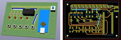
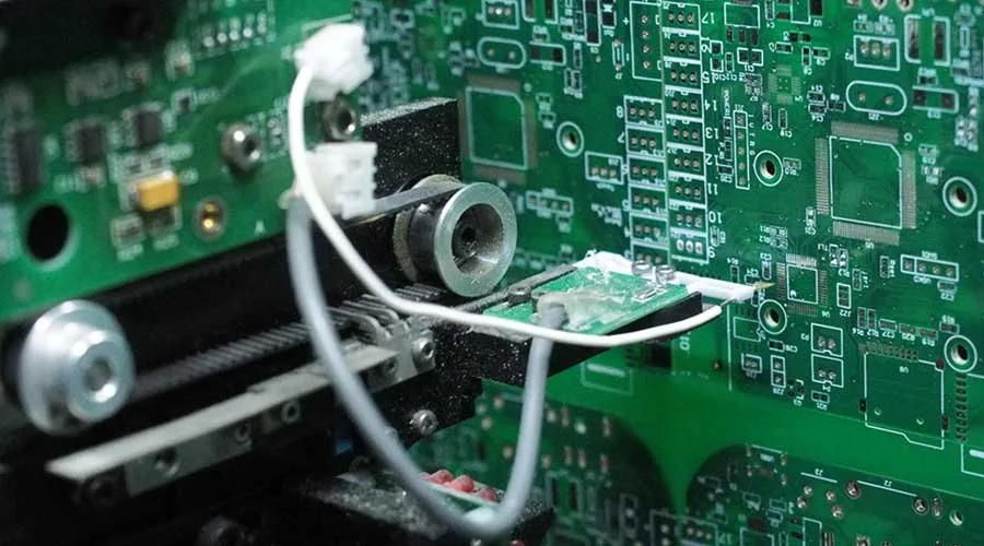
Jumper wires consist of insulated conductive strands soldered between designated pads on the board's surface. They connect separate nets where traces cannot cross without violating routing rules on a single copper layer. In single-sided designs, pads for jumpers appear as enlarged or paired copper areas, facilitating secure attachment. This method suits prototypes and high-volume runs alike, as it avoids complex etching processes. Single-sided PCB jumper wire design integrates these elements early to prevent assembly bottlenecks.
The relevance stems from single-sided PCBs' dominance in budget-constrained sectors. Manufacturing these boards involves simpler etching and plating, reducing lead times and defect rates. Jumper wires extend their utility to moderately complex circuits, such as LED drivers or power supplies. Without them, many designs would require costlier alternatives. Standards like IPC-A-610J outline acceptability criteria for such assemblies, ensuring consistent quality across production.
Electrically, jumper wires carry signals or power with minimal added resistance if sized appropriately. Their placement must account for current demands and thermal dissipation during soldering. Factory insights reveal that jumpers simplify rework compared to trace modifications. This practicality matters in iterative development cycles common among electric engineers.
Key Advantages: Single-Sided PCB Jumper Wire Benefits
One primary benefit lies in cost reduction, as single-sided boards incur lower fabrication expenses than multi-layer options. Jumper wires eliminate the need for additional layers, preserving economic advantages while enabling essential connections. Production scales efficiently, with etching limited to one side and assembly focusing on through-hole or surface soldering. Engineers report savings of up to significant percentages in prototyping phases through this method.
Manufacturing simplicity ranks high among single-sided PCB jumper wire benefits. Factories process these boards with basic equipment, minimizing setup changes and material waste. Jumper addition occurs post-etching, integrating seamlessly into wave or hand soldering flows. This streamlines workflows, especially for high-mix, low-volume runs. Reliability improves when jumpers follow guidelines, reducing failure points from trace overcrowding.
Related Reading: Optimizing Mixed Technology PCB Assembly: A Guide to SMT and Through-Hole Integration
Electrical performance benefits from jumper wires' low inductance in short spans. They maintain signal integrity for DC or low-frequency applications typical of single-sided designs. Mechanical stability enhances durability, as wires bridge gaps without stressing fragile traces. Per IPC-7711/7721D, proper attachment ensures long-term vibration resistance in end-use environments. These factors make jumpers indispensable for factory-driven optimizations.
Single-Sided PCB Jumper Wire Design Considerations
Effective single-sided PCB jumper wire design begins with pad allocation during layout. Pads should exceed standard trace widths to accommodate wire diameter and solder fillet. Spacing prevents bridging during assembly, adhering to clearance rules for voltage levels. Wire gauge selection matches current capacity, avoiding overheating under load. Insulation thickness suits environmental exposure, such as humidity or dust.
Layout software aids visualization by modeling jumpers as top-layer tracks initially. This previews crossings and lengths, optimizing paths before fabrication. Factory standards emphasize symmetrical pad pairs for uniform soldering. Integration with components minimizes shadow effects during reflow if mixed assembly applies. Overall, thoughtful design upholds IPC-A-610J acceptability for production yields.
Thermal management influences jumper selection, as soldering imparts localized heat. Pre-tinned wires reduce dwell times, protecting nearby laminates. Strain relief forms, like gentle bends, prevent fatigue from board flexure. These considerations ensure designs transition smoothly from prototype to volume manufacturing.
Best Practices for Single-Sided PCB Jumper Wire Placement
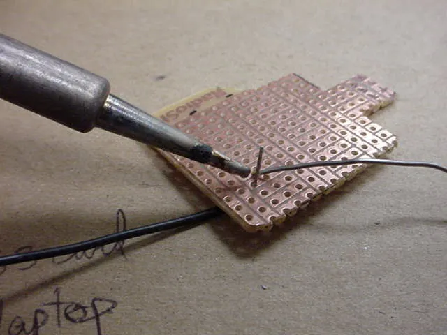
Optimal single-sided PCB jumper wire placement prioritizes straight, non-crossing routes to simplify assembly. Position jumpers parallel to board edges where possible, avoiding high-component density zones. Height control keeps wires flush against the surface, preventing interference with enclosures or connectors. Soldering secures ends fully on pads, forming smooth fillets without excess solder balls.
IPC-7711/7721D provides procedures for attachment, stressing insulation integrity and wire forming. Factories train operators on X-Y routing patterns, which minimize bends and material use. Inspection verifies no shorts via continuity tests post-placement. Documentation labels jumper nets clearly for traceability. These practices boost first-pass yields in production lines.
Hand soldering suits low volumes, while automated dispensers handle insulation for consistency. Post-placement cleaning removes flux residues to avert corrosion. Vibration testing validates mechanical hold in final assemblies. Adhering to these steps aligns with J-STD-001 requirements for soldered joints.
Alternatives to Single-Sided PCB Jumper Wires
While jumper wires excel in simplicity, single-sided PCB jumper wire alternatives exist for specific scenarios. Zero-ohm surface-mount resistors offer compact bridging without added height, suiting automated assembly. However, they demand precise placement and increase component count. Double-sided boards provide etched vias for crossings, eliminating wires entirely but raising costs.
Conductive epoxies serve repair contexts, filling trace gaps without soldering heat. Their resistance suits low-power signals, though not high currents. Upgrading to flexible single-sided variants allows folding for pseudo-crossings, beneficial in compact housings. Each alternative trades jumper wires' flexibility for other attributes, like density or permanence.
Factory evaluations weigh trade-offs: jumpers favor quick iterations, while etched solutions prioritize cleanliness. For most low-complexity designs, jumpers retain superiority in cost and ease. Engineers select based on volume, environment, and performance needs.
Related Reading: Conductive Ink vs. Jumper Wires: Which PCB Trace Repair Method is Best?
Practical Insights from Manufacturing
In production environments, jumper wires facilitate rapid prototyping feedback loops. Engineers iterate designs by swapping wires, testing variants without new boards. Factories observe fewer etch errors since routing focuses on feasible paths. Assembly lines adapt easily, with jumpers added after component population.
Troubleshooting benefits emerge during failure analysis. Replacing a failed jumper restores function faster than trace repairs. Standards-guided inspections catch placement issues early, maintaining quality. These insights underscore jumpers' role in sustainable, efficient workflows.
Conclusion
Jumper wires unlock significant advantages for single-sided PCBs, from cost savings to manufacturing agility. Their integration demands disciplined design and placement to maximize reliability. Standards like IPC-7711/7721D and IPC-A-610J provide the framework for success. Electric engineers benefit by leveraging these practices for robust, economical designs. Ultimately, jumper wires bridge limitations effectively, sustaining single-sided boards' relevance in modern electronics.
FAQs
Q1: What are the main single-sided PCB jumper wire benefits for electric engineers?
A1: Single-sided PCB jumper wire benefits include reduced fabrication costs, simplified routing for trace crossings, and enhanced prototyping flexibility. They maintain electrical performance in low-frequency applications while easing assembly. Factories achieve higher yields through standardized soldering per J-STD-001. Overall, they balance complexity and economy effectively.
Q2: How does single-sided PCB jumper wire placement impact assembly reliability?
A2: Proper single-sided PCB jumper wire placement involves straight routes, flush heights, and secure pad soldering to avoid shorts or fatigue. Factories route in X-Y patterns to minimize stress points. Inspection per IPC-A-610J ensures joint integrity. This approach enhances vibration resistance and long-term durability.
Q3: What single-sided PCB jumper wire design tips improve manufacturability?
A3: In single-sided PCB jumper wire design, allocate oversized pads, select matched wire gauges, and preview crossings in layout tools. Symmetrical pairs aid uniform soldering. Insulation must withstand environments. These steps align with factory processes for seamless production.
Q4: What are viable single-sided PCB jumper wire alternatives and when to use them?
A4: Single-sided PCB jumper wire alternatives include zero-ohm resistors for density or double-sided etching for permanence. Conductive epoxies suit repairs. Choose jumpers for cost-sensitive prototypes, opting for alternatives in high-volume or space-constrained scenarios. Factory trade-offs guide selection.
References
IPC-7711/7721D — Rework, Repair and Modification of Electronic Assemblies. IPC, 2024
IPC-A-610J — Acceptability of Electronic Assemblies. IPC, 2024
J-STD-001 — Requirements for Soldered Electrical and Electronic Assemblies. IPC, 2024


