ALLPCB


Introduction
In the realm of PCB design, high-frequency PCBs pose unique challenges for maintaining signal integrity amid rising data rates and complex routing demands. Electrical engineers often grapple with issues like signal reflections, attenuation, and crosstalk that degrade performance in applications such as telecommunications, radar systems, and high-speed computing. Stacked vias emerge as a strategic solution, enabling compact interconnects that preserve signal quality while supporting multilayer stackups essential for high-frequency operation. These vias, layered directly atop one another, minimize discontinuities and facilitate precise impedance matching, making them ideal for environments where every picosecond counts. This article explores how stacked vias enhance high-frequency PCB design, offering practical insights into their implementation for optimal signal integrity.
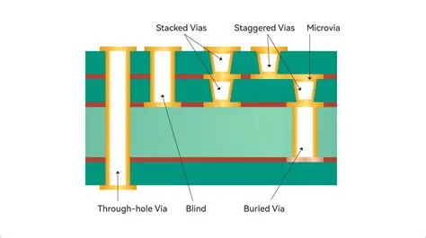
Understanding Stacked Vias in PCB Design
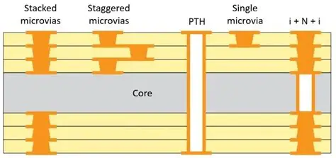
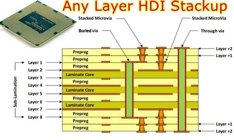
Stacked vias consist of multiple vias aligned vertically through successive layers, typically using blind or buried configurations rather than full through-holes. Unlike staggered vias, which offset each via slightly, stacked vias share the same centerline, creating a continuous conductive path with reduced overall length. This design is particularly prevalent in high-density interconnect (HDI) boards, where space constraints demand efficient layer transitions. In high-frequency PCBs, stacked vias help avoid the long stubs associated with through-vias, which can resonate at microwave frequencies and introduce unwanted reflections. By confining vias to specific layer pairs, engineers achieve tighter control over the interconnect geometry, directly impacting signal propagation characteristics.
The relevance of stacked vias stems from the escalating layer counts in modern high-frequency PCBs, often exceeding 20 layers to accommodate dense routing and shielding. Traditional through-vias traverse the entire board thickness, leading to impedance mismatches and increased inductance that compromise signal integrity. Stacked vias mitigate these by segmenting the connection, allowing each segment to be optimized for minimal parasitic effects. IPC-2226A outlines specific guidelines for such HDI constructions, emphasizing limits on stack height to ensure reliability under thermal stress. For electrical engineers, adopting stacked vias translates to fewer redesign iterations and improved yield in production.
Technical Principles Behind Stacked Vias and Signal Integrity
Signal integrity in high-frequency PCBs hinges on controlling key parameters like characteristic impedance, insertion loss, and return loss across the transmission path. Vias act as critical junctions where these parameters shift due to changes in geometry, introducing discontinuities modeled as lumped elements: inductance from the via barrel, capacitance from the pads, and resistance from plating. In stacked configurations, the shorter effective length per via reduces barrel inductance, which scales with height, thereby minimizing signal reflections quantified by time-domain reflectometry (TDR). Furthermore, precise alignment ensures smooth transitions, preserving the 50-ohm or 100-ohm impedance common in differential pairs for high-frequency signals.
At frequencies above 1 GHz, skin effect confines current to the via walls, amplifying losses if plating quality varies. Stacked vias, often microvias with diameters under 150 microns, benefit from laser drilling and sequential lamination, yielding smoother walls and lower resistance. This setup also supports back-drilling elimination, as blind vias terminate exactly where needed, preventing stub-induced resonances that peak at quarter-wavelength intervals. Impedance matching becomes feasible through pad size optimization and anti-pad adjustments, with simulations revealing return loss improvements exceeding 10 dB compared to through-vias. Electrical engineers leverage these principles to design paths where minimizing signal loss aligns with routing density goals.
Dielectric materials in high-frequency PCBs, characterized by low dissipation factor (Df), interact with via structures to influence propagation delay. Stacked vias embedded in such cores maintain uniform fields, reducing mode conversion in coupled lines. IPC-6018D specifies performance criteria for these boards, including conductor thickness uniformity critical for via plating integrity. The cumulative effect is a transmission line model where stacked vias contribute negligibly to overall skew, essential for multi-gigabit serdes interfaces.
Related Reading: Unlocking Density: A Deep Dive into Stacked Via PCBs for HDI Designs
Impedance Matching and Minimizing Signal Loss with Stacked Vias
Impedance matching forms the cornerstone of signal integrity, ensuring maximum power transfer and minimal reflections in high-frequency PCB traces. Stacked vias disrupt this if not designed carefully, as pad-to-barrel transitions create capacitive loading. Engineers counter this by tapering pad sizes progressively through the stack and employing filled vias for capacitance neutralization, stabilizing the impedance profile. Field solvers confirm that such optimizations keep variations below 5% across a 10 GHz bandwidth, vital for eye diagram closure in high-speed links.
Minimizing signal loss involves addressing conductor, dielectric, and radiation components. Stacked vias shorten the high-loss via path, shifting energy back to low-loss traces sooner. Plating with thicker copper or alloy enhancements further curbs resistive losses, especially under high current densities at RF peaks. In practice, combining stacked vias with embedded ground planes forms stripline or microstrip modes with predictable loss tangents. This synergy reduces insertion loss by optimizing the return path, where ground inductance directly affects common-mode rejection.
For differential signaling, symmetric stacked via pairs maintain balance, suppressing noise coupling. IPC-2221C provides foundational spacing rules that prevent crosstalk amplification through via fields. Overall, these techniques ensure high-frequency PCBs deliver clean signals, even in dense environments.
Best Practices for Implementing Stacked Vias in High-Frequency PCB Design
Successful integration of stacked vias begins with stackup planning, balancing layer count against via aspect ratios typically limited to 1:1 for microvias. Engineers should define via types early—blind for outer layers, buried for inner—to avoid mechanical stress concentrations. Sequential build-up processes enable this, with each lamination step inspected for alignment tolerances under 50 microns. Fabrication partners must qualify per class 3 requirements, verifying plating continuity via cross-section analysis.
Routing strategies prioritize via farms for power but isolate signal vias with ground stitching to contain fields. Simulate early using 3D electromagnetic tools to predict TDR signatures and adjust anti-pads accordingly. For impedance control, reference trace widths to via diameters, ensuring continuity in controlled impedance regions. Thermal management is crucial, as stacked vias concentrate heat; incorporate thermal vias in adjacent planes.
Design rule checks (DRC) enforce minimum clearances, especially between stacked and adjacent vias, to avert shorts during lamination flow. Post-design, perform signal integrity (SI) verification through vector network analyzer (VNA) targets on coupon structures. These practices, rooted in disciplined PCB design, yield robust high-frequency PCBs with superior signal integrity.
Related Reading: Mastering Stacked Via Design: Rules and Best Practices
Design Challenges and Troubleshooting Stacked Vias
Despite advantages, stacked vias introduce challenges like reliability under cyclic thermal loads, where coefficient of thermal expansion (CTE) mismatches cause cracks. Limit stacks to two or three levels, as higher counts risk via pull-out during reflow. X-ray inspection reveals barrel voids early, guiding rework. Signal degradation from misalignment manifests as increased jitter; calibrate drilling for sub-25 micron accuracy.
Crosstalk arises if ground return paths weaken; dense stitching vias around signal stacks restores shielding. For high-frequency operation, resonance from unfilled vias demands conductive epoxy fills. Troubleshooting involves isolating via transitions in simulations, correlating with hardware measurements. Proactive DFM reviews mitigate most issues, ensuring first-pass success.
Conclusion
Stacked vias represent a pivotal advancement in high-frequency PCB design, seamlessly aligning dense interconnects with stringent signal integrity demands. By curtailing stubs, refining impedance matching, and curbing losses, they enable reliable performance at multi-GHz speeds. Electrical engineers benefit from structured guidelines in standards like IPC-2226A, IPC-6018D, and IPC-2221C, fostering designs that withstand real-world rigors. Embracing these techniques minimizes redesigns, accelerates time-to-market, and elevates overall PCB quality. As frequencies climb, stacked vias will remain indispensable for cutting-edge applications.
FAQs
Q1: What role do stacked vias play in maintaining signal integrity on high-frequency PCBs?
A1: Stacked vias enhance signal integrity by providing short, controlled transitions between layers, reducing inductance and reflections compared to through-vias. They support precise impedance matching through optimized pad geometries and eliminate stub resonances, crucial for frequencies above 5 GHz. In PCB design, this minimizes signal loss and preserves eye opening in high-speed links. Following IPC-2226A guidelines ensures reliability in HDI structures.
Q2: How do stacked vias contribute to impedance matching in high-frequency PCB layouts?
A2: Stacked vias facilitate impedance matching by segmenting vertical paths into low-aspect-ratio segments, allowing uniform field distribution. Engineers adjust anti-pad sizes and plating thickness to align via impedance with trace values, typically 50 ohms single-ended. This continuity prevents TDR discontinuities, vital for minimizing signal loss in RF applications. Simulations validate designs before fabrication.
Q3: What are best practices for minimizing signal loss with stacked vias in PCB design?
A3: To minimize signal loss, use blind microvias with conductive fills and limit stack depth to two levels for thermal reliability. Pair with low-Df dielectrics and ground planes for low-inductance returns. IPC-6018D performance specs guide qualification, ensuring plating integrity. Dense stitching reduces radiation losses in high-frequency PCBs.
Q4: When should electrical engineers choose stacked vias over staggered vias for high-frequency PCBs?
A4: Opt for stacked vias in space-constrained, multilayer high-frequency PCBs needing straight vertical paths for optimal signal integrity. They excel in impedance-controlled environments but require precise alignment. Staggered vias suit cost-sensitive designs with looser density. Evaluate via simulation for return loss in PCB design.