 ALLPCB


What Is Sequential Lamination and Why It Matters
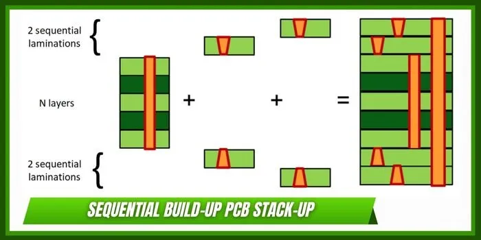
Sequential lamination involves adding one or more layers to a core, drilling and plating vias at intermediate stages, then repeating the process until the final stackup is complete. This method differs from traditional lamination where all layers are pressed together in a single operation. It allows microvias and staggered via patterns that are essential for modern high-speed and compact electronics. PCB design software sequential lamination support helps translate these manufacturing sequences into precise digital models. Without proper software tools, designers may overlook critical constraints such as cumulative registration tolerances or thermal expansion mismatches across build stages. The result is smoother handoff to fabrication and fewer costly revisions.
Technical Principles of Sequential Lamination in PCB Design
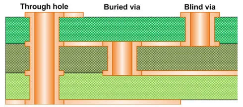
In sequential lamination each build stage requires definition of the layer stack, via types, and plating processes. Microvias formed by laser drilling connect adjacent layers while buried vias span multiple internal layers before outer layers are added. Software must track the sequence of these operations to generate accurate drill files and layer-specific artwork. Registration between stages becomes critical because each lamination cycle introduces potential misalignment. Industry standards such as IPC-2221 provide guidelines for design considerations including via aspect ratios and material selection that influence sequential builds. Proper implementation ensures the final board meets performance requirements for impedance and thermal management.
Design platforms differ in how they represent these staged processes. Some allow users to define multiple lamination cycles with associated via lists and copper weights for each stage. Others rely on manual annotations or external documentation to convey the build sequence to the fabricator. The ability to simulate cumulative effects such as warpage or stress from repeated thermal cycles adds further value during the design phase.
Related Reading: Unlocking HDI Potential: Mastering Sequential Lamination in PCB Design
Software Capabilities for Sequential Lamination
Effective PCB design software sequential lamination features include flexible stackup editors that accommodate variable layer counts per build stage. Users need tools to assign specific via types to individual lamination steps and verify that drill diameters and capture pads comply with manufacturing limits. Integration with signal integrity analysis helps confirm that via transitions do not degrade high-speed performance. Export functions should generate stage-specific Gerber or ODB++ files that fabricators can use directly. Comparison of available tools often centers on the depth of stackup modeling, ease of via mapping across stages, and the robustness of design rule checks tailored to sequential processes.
Some platforms excel at visual representation of the build sequence, allowing designers to step through each lamination cycle interactively. Others provide stronger automation for generating manufacturing documentation but require more manual effort to define the sequence initially. The choice depends on project complexity, with high-layer-count boards benefiting from more sophisticated modeling. Engineers also consider how well the software handles material libraries that include properties relevant to multiple lamination cycles.
Related Reading: The Engineer's Guide to Sequential Lamination: Materials, Processes, and Best Practices
Best Practices for Using Design Software in Sequential Lamination Projects
Begin by defining the complete layer stack and via strategy early in the design cycle while consulting relevant manufacturing guidelines. Apply consistent design rules that account for the tighter tolerances typical of sequential builds. Validate the model by generating reports that list each lamination stage and its associated features. Collaboration with the fabrication team remains essential to confirm that software outputs align with actual process capabilities. Regular reviews of stackup symmetry and copper balance help minimize warpage risks across multiple press cycles.
Adherence to standards such as IPC-6012E supports qualification of the finished boards and informs software rule settings. Documentation generated by the software should clearly communicate the build sequence without ambiguity. Testing impedance structures at different stages provides additional confidence before committing to production. These practices reduce the likelihood of issues that arise only after boards reach the assembly line.
Conclusion
Sequential lamination demands precise planning that modern PCB design software can facilitate when the right capabilities are present. Comparing tools on stackup flexibility, via management, and documentation output helps engineers select platforms suited to their projects. Following established design principles and industry standards ensures reliable results from concept through fabrication. Investment in appropriate software features ultimately supports higher yields and more compact, high-performance boards.
FAQs
Q1: What features define effective PCB design software sequential lamination support?
A1: Robust stackup editors, stage-specific via assignment, and automated documentation generation rank among the most important capabilities. These functions allow designers to model the build process accurately and produce files that match fabrication requirements. Proper implementation reduces errors related to registration and material behavior across multiple lamination cycles.
Q2: How does sequential lamination differ from standard multilayer PCB design in software tools?
A2: Sequential lamination requires explicit definition of intermediate build stages and associated via structures, whereas standard multilayer designs typically assume a single lamination operation. Software that handles sequential processes provides tools to track cumulative tolerances and generate phased manufacturing outputs. This added functionality supports denser interconnects but increases the complexity of the design workflow.
Q3: Why should engineers evaluate PCB design software sequential lamination options before starting high-density projects?
A3: Early evaluation ensures the chosen platform can represent the intended build sequence without excessive manual workarounds. Tools with strong sequential support improve collaboration with fabricators and help meet performance targets for signal integrity and thermal characteristics. Selecting appropriate software ultimately contributes to smoother project execution and fewer revisions.
Q4: What role do industry standards play when using software for sequential lamination designs?
A4: Standards guide the setting of design rules and acceptance criteria that software can enforce during layout. They inform decisions on via dimensions, material choices, and qualification testing that apply across lamination stages. Consistent reference to these standards helps maintain quality and interoperability between design and manufacturing teams.
References
IPC-2221 — Generic Standard on Printed Board Design. IPC
IPC-6012E — Qualification and Performance Specification for Rigid Printed Boards. IPC, 2017
IPC-A-600K — Acceptability of Printed Boards. IPC, 2020





