 ALLPCB


Introduction
Sequential lamination represents a critical advancement in PCB manufacturing for producing high-density interconnect boards. This process enables the creation of complex multilayer structures with blind and buried vias, which are essential for modern electronics demanding high performance and compactness. Engineers must understand sequential lamination to optimize designs for reliability and manufacturability. Factory operations rely on precise control of materials and cycles to avoid defects like delamination or warpage. By mastering PCB lamination materials and processes, teams can achieve superior signal integrity and thermal management. This guide provides factory-driven insights tailored for electrical engineers navigating these challenges.
What Is Sequential Lamination and Why It Matters
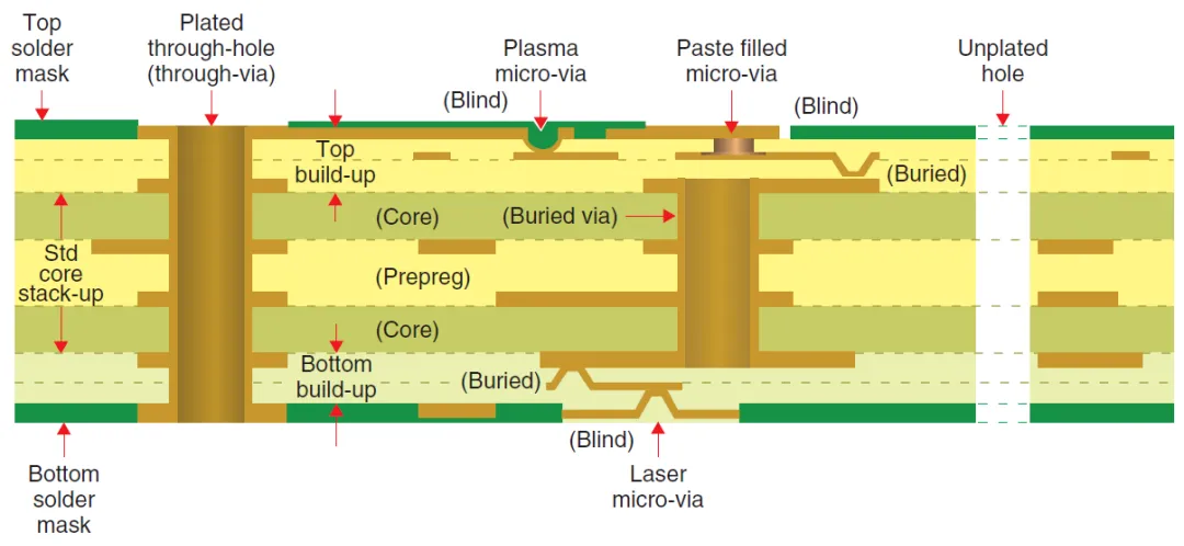
Sequential lamination builds multilayer PCBs through multiple lamination cycles, typically two or more, rather than a single press. Subcomposites or subsets of copper foils, cores, and prepregs are fabricated separately, then bonded progressively with additional dielectric layers. This contrasts with standard lamination, allowing vias to connect specific layers without penetrating the entire stack. In high-layer-count boards, it supports stacked microvias and staggered configurations critical for HDI designs. The process matters because it enables denser routing and shorter signal paths, reducing latency in applications like telecommunications and computing. Factory throughput increases with optimized cycles, but poor execution leads to yield losses from misalignment or stress buildup.
Key Technical Principles of Sequential Lamination
PCB Lamination Materials
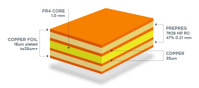
Selecting appropriate PCB lamination materials is foundational for sequential builds, as they must endure repeated thermal and mechanical stresses. Cores provide structural integrity, while prepregs serve as dielectrics with resin that flows to fill gaps and bond layers during pressing. Materials require low coefficient of thermal expansion (CTE) mismatch between copper (around 17 ppm/°C) and resin (60-80 ppm/°C below Tg, higher above), along with high glass transition temperature (Tg) for stability. Thin glass styles and sufficient resin content prevent voids, ensuring uniform thickness. Factory processes demand materials with consistent flow across cycles to maintain layer registration. Adherence to IPC-4101 ensures laminates and prepregs meet qualification for rigid and multilayer boards.
The Sequential Lamination Process
The process begins with fabricating sub-stacks: inner layers are imaged, etched, drilled for buried vias, and plated. Oxide treatments enhance adhesion on plated copper before stacking with prepregs and foils using alignment pins. Panels enter a vacuum-assisted press where heat softens the resin, pressure bonds layers, and controlled cooling solidifies the structure. Subsequent cycles repeat drilling, plating microvias, and lamination on the growing stack. Each cycle introduces potential shrinkage, so precise registration is vital. This iterative approach supports complex via structures but requires meticulous handling to preserve flatness.
Sequential Lamination Temperature Profile
The sequential lamination temperature profile follows a ramp-up to exceed the resin's Tg, allowing flow and cure, followed by a dwell and gradual cool-down under pressure. High temperatures melt epoxy in prepregs, while pressures around 250 psi ensure intimate contact without voids. Cooling rates must be controlled to minimize thermal gradients that cause warpage. Multiple cycles demand materials stable across repeated profiles, avoiding degradation. Factories monitor profiles to match material specifications, preventing resin pull-off or delamination. This profile directly influences Z-axis expansion, where dielectrics grow faster than copper above Tg.
PCB Manufacturing Best Practices for Sequential Lamination
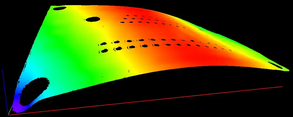
Limit lamination cycles to two or three to balance complexity with yield, as each adds cost and risk of misalignment. Design symmetric stackups to counter CTE-induced warpage, balancing copper distribution across layers. Use vacuum lamination presses for void-free bonding, especially with low-flow prepregs in buildup films. Maximize retained copper on bonding surfaces to promote even resin distribution and reduce stress concentrations. Pre-treat surfaces with high-adhesion oxides and control moisture content below critical levels to prevent pops or cracks. Post-lamination, inspect for warpage using dial gauges and adjust via scaling factors in design files.
Incorporate heat sinks like aluminum plates during pressing for uniform heat transfer, mitigating bow in thick panels. Select prepregs with optimized resin content: lower for subsets to limit expansion, higher for dielectrics to distribute stress. Perform stackup analysis early, simulating thermal excursions per IPC-6012 performance specs. For blind via fills, ensure resin flows adequately without overfilling, which traps air. These PCB manufacturing best practices align factory processes with design intent, enhancing reliability.
Common Challenges and Troubleshooting in Sequential Lamination
Warpage emerges as a primary issue from asymmetric stacks or CTE mismatches during cool-down, measurable up to several mils in high-layer boards. Voids form if resin flow is insufficient, often traceable to inadequate prepreg quantity or air entrapment; X-ray inspection reveals them early. Delamination risks rise with repeated cycles due to weakened oxide bonds or moisture; bake panels pre-lamination to mitigate. Microvia reliability suffers from Z-axis copper extension under pressure, addressed by plating controls. Factories troubleshoot via cross-section analysis, adjusting parameters iteratively. Proactive design reviews prevent most defects.
Conclusion
Sequential lamination unlocks advanced PCB capabilities through careful materials selection, precise processes, and rigorous best practices. Engineers benefit from understanding PCB lamination materials' role in CTE matching and Tg stability, alongside controlled temperature profiles for bonding. Factory success hinges on limiting cycles, symmetric designs, and standard adherence like IPC-4101 and IPC-6012. Implementing these strategies minimizes warpage, voids, and delamination while maximizing density. For electrical engineers, this knowledge ensures designs transition seamlessly to production. Prioritizing these elements drives reliable, high-performance boards.
FAQs
Q1: What are the key PCB lamination materials used in sequential lamination?
A1: PCB lamination materials include cores for rigidity and prepregs as dielectrics with controlled resin flow. High Tg materials prevent degradation across cycles, while low CTE variants match copper expansion. Factories select thin glass styles for uniform filling. These ensure adhesion and minimal voids in HDI builds. Proper selection per IPC-4101 supports multiple laminations without reliability loss.
Q2: How does the sequential lamination temperature profile affect PCB quality?
A2: The sequential lamination temperature profile ramps above Tg for resin flow, holds for cure, and cools slowly to reduce stress. Mismanaged profiles cause warpage from expansion differences. Pressures aid bonding but demand vacuum to avoid voids. Factories tailor profiles to materials for consistent Z-axis control. This maintains layer integrity in complex stacks.
Q3: What are essential PCB manufacturing best practices for sequential lamination?
A3: Key PCB manufacturing best practices include 2-3 cycles maximum, symmetric stackups, and CTE-matched materials. Vacuum pressing eliminates voids, while oxide treatments boost adhesion. Control moisture and use alignment pins for registration. Inspect warpage post-cycle and simulate thermal behavior. These steps align with IPC-6012 for high yields.
Q4: How can engineers control warpage in sequential lamination processes?
A4: Control warpage by balancing copper distribution and using heat sinks in presses for even cooling. Symmetric designs counter CTE effects across layers. Material choices with low Z-axis expansion minimize bow. Factories measure with gauges and apply scaling. Pre-lamination bakes reduce moisture-induced issues. This ensures flat panels for assembly.
References
IPC-4101E — Specification for Base Materials for Rigid and Multilayer Printed Boards. IPC, 2017
IPC-6012DS — Qualification and Performance Specification for Rigid Printed Boards. IPC, 2020
IPC-A-600K — Acceptability of Printed Boards. IPC, 2020


