 ALLPCB


In the fast-evolving world of electronics, High-Density Interconnect (HDI) PCBs have become a cornerstone for creating compact, high-performance devices. A key technique in HDI PCB manufacturing is sequential lamination, which allows for intricate designs with microvias and multiple layers. If you're looking to understand HDI PCB sequential lamination design rules, sequential lamination for microvias, or high-density interconnect PCB manufacturing techniques, you're in the right place. This blog dives deep into mastering sequential lamination to unlock the full potential of HDI designs, offering practical insights and actionable tips for engineers and designers.
What Is Sequential Lamination in HDI PCB Design?
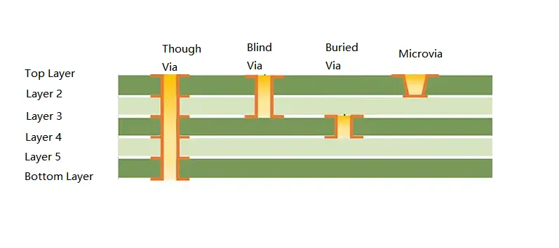
Sequential lamination is a manufacturing process used in HDI PCBs to build complex, multi-layer boards by adding layers in stages. Unlike traditional lamination, where all layers are stacked and pressed together at once, sequential lamination involves bonding subsets of layers (or cores) step by step. This method enables the creation of intricate interconnects, such as microvias, which are tiny holes drilled with lasers to connect layers in a high-density layout.
This process is essential for modern electronics, where space is limited, and performance demands are high. Think of smartphones, wearables, and medical devices—HDI PCBs with sequential lamination make their compact, powerful designs possible. In this guide, we'll explore how sequential lamination works, the design rules to follow, and best practices to ensure reliable, high-quality boards.
Why Sequential Lamination Matters for HDI PCBs
HDI PCBs are defined by their high component density, fine lines, and small vias. Sequential lamination plays a critical role in achieving these features by allowing manufacturers to create boards with 6, 8, or even more layers while maintaining precision. Here are some key benefits:
- Increased Density: Sequential lamination supports microvias, which are typically 0.1 mm or smaller in diameter, enabling more connections in a smaller area compared to traditional through-hole vias.
- Improved Signal Integrity: By reducing the length of interconnects, sequential lamination helps maintain signal speeds, often supporting frequencies above 1 GHz in high-speed applications.
- Flexibility in Design: Designers can stack microvias in various configurations (stacked or staggered), optimizing space and performance for specific needs.
Without sequential lamination, achieving the miniaturization and performance required for modern devices would be nearly impossible. However, this process comes with challenges, which is why understanding design rules and manufacturing techniques is so important.
Understanding the Sequential Lamination Process
The sequential lamination process involves several steps, each carefully controlled to ensure the integrity of the board. Here's a simplified breakdown:
- Core Preparation: The process starts with a core layer, often made of a thin dielectric material like FR-4 or a high-performance laminate, with copper foil on both sides.
- First Lamination: Additional dielectric and copper layers are added to the core and bonded under heat and pressure. This forms a subset of the final board.
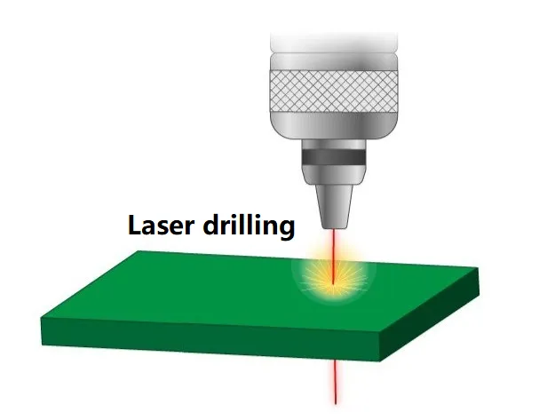
- Microvia Drilling: Lasers drill tiny holes (microvias) through the newly added layers to create connections. These holes are often less than 0.15 mm in diameter for precision.
- Plating: The microvias are plated with copper to establish electrical connections between layers.
- Repeat Cycles: Additional layers are laminated, drilled, and plated in sequence until the desired layer count is achieved.
- Final Processing: The board undergoes surface finishing, testing, and inspection to ensure quality.
This step-by-step approach allows for greater control over layer alignment and via placement, which is critical for HDI designs. However, each cycle of lamination adds complexity, making adherence to design rules essential.
HDI PCB Sequential Lamination Design Rules
Designing for sequential lamination requires careful planning to avoid manufacturing issues and ensure reliability. Below are some critical design rules to follow when working on HDI PCBs with sequential lamination:
1. Microvia Aspect Ratio
The aspect ratio of a microvia (depth to diameter) should typically be kept at 0.75:1 or lower. For example, a microvia with a diameter of 0.1 mm should not exceed a depth of 0.075 mm. This prevents issues during plating, where copper may not deposit evenly in deeper holes, leading to weak connections.
2. Via Stacking and Staggering
In HDI designs, microvias can be stacked directly on top of each other or staggered (offset between layers). Stacked vias save space but are harder to manufacture and may require filled vias for stability. Staggered vias are more reliable but take up more room. Choose based on your board's density and performance needs, ensuring at least a 0.2 mm offset for staggered configurations.
3. Layer Count and Material Selection
Sequential lamination often involves 6 to 12 layers or more. Use thin dielectric materials (0.05 mm to 0.1 mm thick) to keep the board compact. Select materials with low dielectric constants (Dk around 3.5 to 4.0) for high-speed signals to minimize signal loss.
4. Trace Width and Spacing
HDI designs often feature trace widths and spacing as small as 0.075 mm (3 mils). Ensure your design software accounts for manufacturing tolerances, typically ±0.025 mm, to avoid shorts or breaks during production.
5. Pad Size for Microvias
Microvia pads should be at least 0.2 mm larger than the via diameter to ensure proper alignment and connection. For a 0.1 mm via, use a pad diameter of at least 0.3 mm.
Following these rules minimizes risks like delamination, misalignment, or electrical failures. Always collaborate with your manufacturing partner to confirm their specific capabilities and constraints before finalizing your design.
Sequential Lamination for Microvias: Key Considerations
Microvias are a defining feature of HDI PCBs, and sequential lamination is the process that makes them possible. Here are some important factors to consider when designing with microvias in a sequential lamination workflow:
- Laser Drilling Precision: Microvias are created using laser drilling, which offers high accuracy but requires clean dielectric surfaces. Contamination or uneven material can lead to defective vias, so ensure your design specifies high-quality laminates.
- Copper Filling: Some designs require microvias to be filled with copper to improve thermal and mechanical stability, especially for stacked vias. This process adds cost and complexity, so evaluate if it’s necessary for your application.
- Thermal Management: Microvias have limited current-carrying capacity due to their small size. For high-power applications, use multiple vias in parallel to distribute current and prevent overheating.
By addressing these considerations, you can ensure that microvias in your HDI PCB are both functional and reliable, even in demanding environments.
Best Practices in High-Density Interconnect PCB Manufacturing
Manufacturing HDI PCBs with sequential lamination requires precision and attention to detail. Here are some best practices to optimize the process and achieve high-quality results:
1. Collaborate Early with Manufacturers
Engage with your PCB fabrication partner during the design phase. Share your layer stackup, via requirements, and material preferences to confirm they align with their equipment and processes. This can prevent costly redesigns or delays.
2. Optimize Stackup Design
Plan your layer stackup to balance signal integrity and manufacturability. For example, place high-speed signal layers near the top or bottom of the stack to minimize interference, and use ground planes to shield sensitive traces. A typical 8-layer HDI stackup might include 2 signal layers, 2 ground planes, and 4 power or mixed layers.
3. Use Advanced Simulation Tools
Before manufacturing, simulate your design for signal integrity and thermal performance. Tools can predict impedance mismatches (target around 50 ohms for most high-speed signals) and highlight areas of excessive heat buildup, allowing you to adjust your layout accordingly.
4. Test for Reliability
After manufacturing, perform thorough testing, including micro-section analysis to inspect via quality and layer alignment. Electrical testing should verify that impedance values fall within ±10% of the target, ensuring consistent performance.
5. Minimize Lamination Cycles
Each lamination cycle increases the risk of misalignment or material stress. Group layers strategically to reduce the number of cycles, balancing cost and complexity. For instance, a 10-layer board might be built in 3 lamination steps instead of 5 with careful planning.
These practices help ensure that your HDI PCB not only meets design specifications but also performs reliably in real-world applications.
Challenges in Sequential Lamination and How to Overcome Them
While sequential lamination offers incredible benefits, it also presents challenges that designers and manufacturers must address. Here are some common issues and solutions:
- Layer Misalignment: Repeated lamination cycles can cause layers to shift, leading to misaligned vias. Solution: Use precise registration systems and fiducial markers during manufacturing to maintain alignment within 0.05 mm.
- Delamination: Poor bonding between layers can cause separation under thermal stress. Solution: Select compatible materials with similar coefficients of thermal expansion (CTE, ideally around 15-20 ppm/°C) and control lamination temperature and pressure.
- Cost and Time: Sequential lamination is more expensive and time-consuming than standard processes due to multiple cycles. Solution: Optimize your design to reduce layer count or lamination steps where possible without compromising performance.
By anticipating these challenges and planning accordingly, you can achieve a smoother manufacturing process and a more reliable end product.
Conclusion: Elevate Your HDI Designs with Sequential Lamination
Sequential lamination is a powerful technique that unlocks the full potential of HDI PCBs, enabling the creation of compact, high-performance electronics. By mastering HDI PCB sequential lamination design rules, understanding sequential lamination for microvias, and following best practices in high-density interconnect PCB manufacturing, you can design boards that meet the demands of modern applications.
From optimizing microvia aspect ratios to collaborating with manufacturers, every step in the process plays a role in ensuring quality and reliability. As technology continues to push the boundaries of miniaturization, sequential lamination will remain a critical skill for engineers and designers. With the insights and tips shared in this guide, you're well-equipped to tackle your next HDI project with confidence.


