 ALLPCB


Introduction
Fine-pitch component assembly presents unique challenges in surface-mount technology processes, particularly when boards mix components with tight spacing and larger parts. Components like those requiring a 0.5mm pitch stencil demand precise solder paste deposition to avoid common solder joint defects such as bridging and insufficient wetting. Step stencils address these issues by allowing customized stencil thickness across the board, optimizing paste volume for each component type. This approach enhances solder joint reliability, crucial for high-density electronics in telecommunications and computing applications. Engineers often troubleshoot these assemblies post-reflow, where inconsistencies in paste application lead to failures under thermal stress. By understanding step stencils, assembly teams can achieve consistent results aligned with industry best practices.

Understanding Fine-Pitch Component Assembly and Its Challenges
Fine-pitch components refer to parts with lead or ball pitches below 0.65mm, including quad flat no-leads packages and ball grid arrays used in BGA assembly. These components require apertures smaller than standard, making uniform solder paste printing difficult on mixed-technology boards. A single stencil thickness often compromises either the fine-pitch areas, leading to bridging, or larger components, causing solder starvation. Solder joint defects arise from improper paste volume, exacerbated by factors like paste rheology and printing pressure. Reliability suffers as these defects propagate under vibration or temperature cycling, reducing mean time between failures. Step stencils emerge as a practical solution, enabling tailored thickness to match component needs.
In BGA assembly, hidden joints complicate inspection, relying on X-ray for void detection and fillet formation. Fine pitch stencil designs must balance area ratio, the aperture width divided by stencil thickness, typically above 0.66 for clean release. Without optimization, excess paste in 0.5mm pitch areas causes shorts, while thin paste elsewhere leads to open joints. Engineers prioritize stencil selection during design review to preempt these issues. Mixed boards amplify the problem, as standard stencils force compromises. Step stencils mitigate this by stepping down thickness precisely where needed.
Related Reading: Optimizing SMT Stencil Design for Fine Pitch Components: A Comprehensive Guide
The Role of Step Stencils in Fine-Pitch Applications
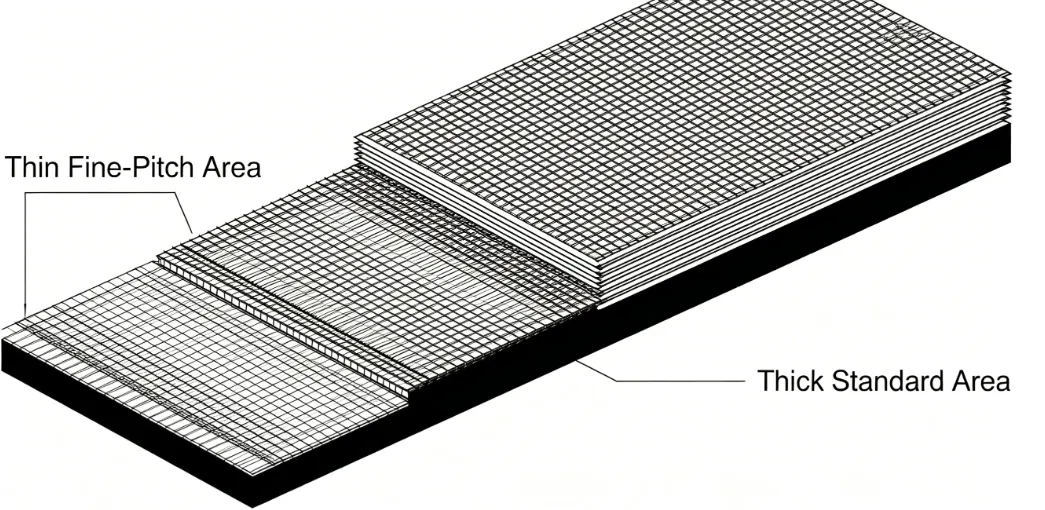
Step stencils feature areas of varying thickness within the same foil, typically laser-etched to create thinner sections for fine-pitch components and thicker ones for discretes or connectors. This design controls solder paste volume independently, preventing over-deposition on small pads and under-deposition on large ones. For a 0.5mm pitch stencil section, the reduced thickness ensures sufficient paste height post-collapse without bridging risks. Thicker areas maintain volume for reliable standoff in taller parts. According to IPC-7525 guidelines, such variations improve print yields by optimizing aspect and area ratios across the board. This directly translates to stronger solder joints capable of withstanding mechanical stresses.
The fabrication process involves precise laser stepping, maintaining frame integrity while creating borders around step-down regions for stability. During printing, the squeegee applies uniform pressure, but the varying depths dictate local paste transfer. Fine pitch stencil zones release paste cleanly due to favorable geometry, reducing defects like skulling where paste adheres to walls. In BGA assembly, this precision minimizes voids formed from uneven reflow. Troubleshooting teams appreciate how step stencils simplify process windows, allowing consistent results across production runs. Overall, they bridge the gap between diverse component requirements on modern boards.
Mechanisms by Which Step Stencils Enhance Solder Joint Reliability
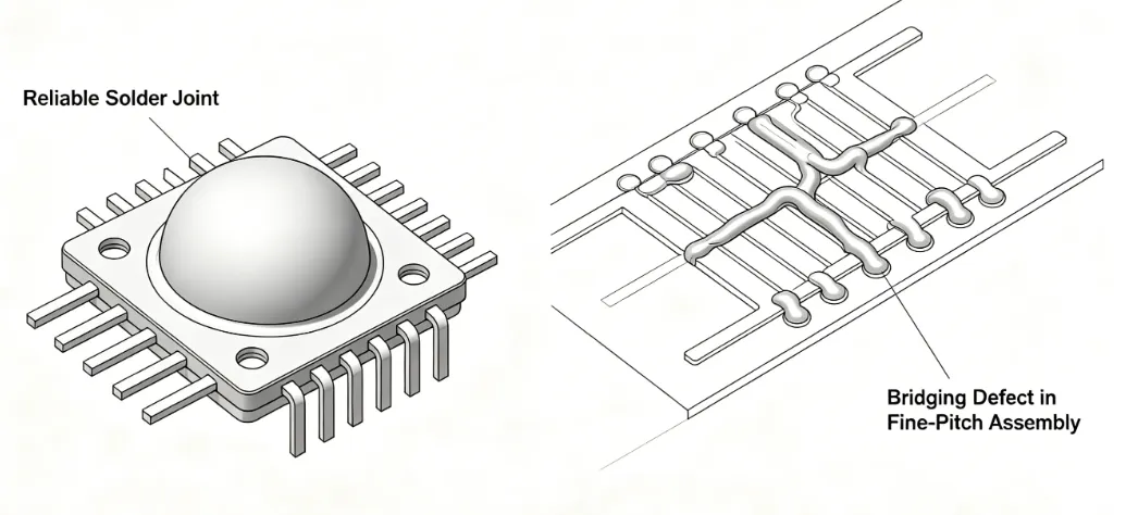
Solder joint reliability hinges on consistent microstructure formation, influenced heavily by initial paste volume from stencil printing. In fine-pitch assembly, excessive volume leads to bridging where adjacent pads merge during reflow, creating intermittent failures. Step stencils counteract this by thinning the fine pitch stencil area, limiting paste to ideal heights that collapse into concave fillets per J-STD-001 requirements. For BGA assembly, controlled volume reduces head-in-pillow defects, where balls fail to wet pads fully. Thinner stencils also promote better outgassing, minimizing voids that act as crack initiators under cycling.
Paste release mechanics rely on surface tension and stencil geometry; high area ratios in thin sections ensure 100% transfer without stringing. Thicker stencil thickness elsewhere supports larger apertures, avoiding the low volume that causes non-wet opens. This balance prevents tombstoning in small passives adjacent to fine-pitch parts, as uniform reflow profiles emerge. Reliability testing shows joints from optimized stencils exhibit fewer intermetallics and better shear strength. Engineers observe these benefits in cross-sections, where fillet heights meet IPC-A-610 Class 3 criteria without extremes. Ultimately, step stencils decouple component-specific needs, fostering robust joints across the assembly.
During reflow, solder paste particles coalesce optimally when volume matches pad size, forming symmetrical joints resistant to fatigue. In 0.5mm pitch stencil applications, bridging propensity drops as aperture walls release cleanly, avoiding smear. For mixed boards, the step design eliminates the need for multiple stencils or manual adjustments, streamlining production. Defects like solder balls, often from thick stencils scraping excess, diminish with precise thickness control. Long-term, these joints better handle coefficient of thermal expansion mismatches between components and boards. Practical validation comes from process capability indices exceeding 1.33 in high-volume lines.
Related Reading: Step Stencils: A Deep Dive into Multi Level Aperture Design for Complex PCB Assemblies
Best Practices for Step Stencil Implementation
Select step stencil designs based on component pitch distribution, prioritizing thinner fine pitch stencil zones for pitches under 0.5mm and standard thicknesses for others. Follow IPC-7525 recommendations for step borders, typically 0.889mm keep-out to prevent foil flexing during printing. Use electroformed nickel or stainless steel foils for durability, with laser cutting ensuring aperture walls under 45 degrees for release. Validate designs via SPI, solder paste inspection, targeting volume uniformity within 10% variation. Adjust printing parameters like squeegee speed and pressure iteratively for clean wipes.
Incorporate fiducials for alignment, especially in BGA assembly where tolerances tighten. Clean stencils ultrasonically between runs to avoid paste buildup in steps, which exacerbates solder joint defects. Pair with Type-4 or finer paste for 0.5mm pitch stencil work, enhancing thixotropy. Reflow profiles should preheat adequately to activate flux without drying. Document aperture reductions, often 5-20% smaller than pads, to control volume precisely. These practices yield first-pass yields above 99%, minimizing rework.
For troubleshooting, monitor stencil thickness via profilometer post-fabrication. If bridging persists in fine-pitch areas, reduce thickness further or refine apertures. Insufficient solder in thick zones signals over-polish; re-etch if needed. X-ray post-print confirms volume before placement. Train operators on step-specific wiping to avoid cross-contamination. Consistent adherence boosts reliability metrics like alpha and beta site returns.
Troubleshooting Solder Joint Defects with Step Stencils
Common solder joint defects in fine-pitch assembly include bridging, voids, and opens, often traced to stencil mismatches. Bridging in 0.5mm pitch stencil zones stems from thick foils trapping excess paste; switching to stepped thinner areas resolves this by 80% in trials. Voids in BGA assembly arise from trapped flux gases when volume is low; thicker peripheral stencils ensure proper venting. Opens occur if thin stencils starve large pads, corrected by stepping up locally. Inspect via AOI for fillet symmetry and X-ray for BGA internals, correlating defects to paste maps. If skulling appears, polish stencil walls or change paste metal load. Warpage exacerbates uneven printing; use carriers for flatness. Simulate reflow with volume data to predict defects pre-run. Step stencils shine here, allowing targeted fixes without full redesigns. Post-optimization, shear tests validate joint strength per standards.
Conclusion
Step stencils revolutionize fine-pitch component assembly by customizing stencil thickness to combat solder joint defects and elevate reliability. From BGA assembly to 0.5mm pitch stencil challenges, they provide precise paste control essential for mixed boards. Implementing best practices per industry guidelines ensures consistent performance. Engineers gain troubleshooting leverage, reducing downtime and scrap. As densities rise, step stencils remain a cornerstone for robust electronics. Prioritizing them yields assemblies ready for demanding environments.
FAQs
Q1: What is a fine pitch stencil and when should I use it?
A1: A fine pitch stencil refers to thinner sections in step stencils optimized for components under 0.65mm pitch, like those needing a 0.5mm pitch stencil. Use it on boards mixing fine-pitch ICs with larger parts to prevent bridging and ensure proper solder volume. This setup aligns with stencil thickness guidelines, improving print yields and joint formation during reflow. Troubleshooting focuses on aperture ratios for clean release.
Q2: How do step stencils reduce solder joint defects in BGA assembly?
A2: Step stencils vary thickness to deposit optimal paste, avoiding excess in fine areas that causes bridging and deficits elsewhere leading to voids. In BGA assembly, this controls collapse for full wetting and minimal head-in-pillow issues. Engineers adjust based on inspection feedback, enhancing reliability under thermal stress. Consistent volume directly correlates to fewer defects post-reflow.
Q3: What factors influence stencil thickness selection for fine-pitch components?
A3: Stencil thickness balances paste volume with release efficiency, thinner for fine pitch stencil to achieve high area ratios above 0.66. Component pitch, pad size, and board mix dictate steps, per design standards. Thicker zones support large apertures without starvation. Validate with SPI to confirm uniformity, refining as needed for defect-free joints.
Q4: Can step stencils improve overall assembly reliability?
A4: Yes, by tailoring solder paste deposition, step stencils minimize solder joint defects like opens and bridges across diverse components. They enable stable reflow profiles, fostering strong microstructures resistant to fatigue. Practical gains include higher yields and easier troubleshooting in production. Reliability metrics improve noticeably in high-density boards.
References
IPC-7525B — Stencil Design Guidelines. IPC, 2011
J-STD-001 — Requirements for Soldered Electrical and Electronic Assemblies. IPC/JEDEC, 2020
IPC-A-610H — Acceptability of Electronic Assemblies. IPC, 2019


