 ALLPCB


Introduction
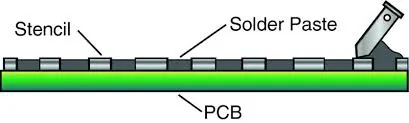
In surface mount technology assembly, solder paste printing remains a critical step that directly impacts overall yield and reliability. Stencils define precise apertures where solder paste deposits form on PCB pads, but challenges like incomplete release and inconsistent transfer efficiency often arise, especially with fine-pitch components. Stencil nano-coatings address these issues by applying ultra-thin layers that optimize aperture surface treatment, leading to superior stencil performance. This technology enhances solder paste transfer efficiency, reduces defects, and supports higher production speeds. Engineers troubleshooting print quality will find nano-coatings particularly valuable for maintaining consistent brick heights and minimizing bridging. As component miniaturization advances, understanding stencil nano-coatings becomes essential for reliable SMT processes.
What Are Stencil Nano-Coatings and Why Do They Matter?
Stencil nano-coatings consist of molecular or ceramic-based films applied to the interior walls and surfaces of SMT stencils, typically at thicknesses below 100 nanometers. These coatings create a low-surface-energy, hydrophobic barrier that repels the flux in solder paste, preventing adhesion to aperture walls. Without such treatments, paste can stick, leading to low transfer volumes and high variability in deposits. In high-volume production, this results in frequent cleaning cycles and yield losses. Nano-coatings improve aperture surface treatment, allowing stencils to handle finer features and thicker foils while upholding solder paste transfer efficiency. For electrical engineers, this means fewer process adjustments and better compliance with assembly tolerances.
The relevance grows with shrinking component sizes, such as 01005 passives or 0.3 mm pitch BGAs, where traditional stencils struggle. Poor stencil performance manifests as insufficient paste volume, tombstoning, or bridging during reflow. Nano-coatings mitigate these by promoting clean snap-off during printing, ensuring uniform deposits. They extend stencil life and reduce downtime, critical for troubleshooting intermittent defects. Overall, integrating stencil nano-coatings elevates SMT stencil reliability in demanding applications.
Technical Principles Behind Nano-Coatings
Nano-coatings function through surface modification that alters wettability and friction at the microscale. Solder paste, a mixture of metal particles and flux, tends to wet metal stencil walls due to flux's polarity, leaving residue that skews subsequent prints. Hydrophobic nano-layers counteract this by reducing contact angle hysteresis, enabling flux to bead up and release cleanly. This principle directly boosts solder paste transfer efficiency, particularly in apertures with low area ratios. Area ratio, defined as aperture area divided by the product of perimeter and foil thickness, guides design per IPC-7525 guidelines; coatings effectively lower the minimum viable ratio from around 0.66 to enable finer features.
Two primary coating types exist: self-assembled monolayers, which form organized chemical bonds on the stencil surface, and ceramic-infused films that provide durable inorganic protection. Both minimize flux retention on walls, yielding consistent volume transfer across print cycles. Engineers observe improved coefficient of variation in deposit heights, as the coating maintains aperture geometry integrity over time. During the print stroke, reduced shear forces prevent paste smearing, preserving brick profiles. These mechanisms align with IPC-7527 criteria for solder paste printing acceptability, emphasizing uniform deposition.
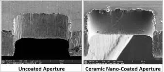
Surface tension dynamics play a key role; untreated apertures trap air pockets or flux films, hindering complete filling and release. Nano-coatings promote laminar flow and rapid evacuation, enhancing fill factors. For troubleshooting, profilometers reveal smoother post-print walls on coated stencils, correlating to higher first-pass yields. Thermal stability ensures performance through repeated cleanings, as the films resist abrasion from wipes or sprays.
Practical Solutions and Best Practices for Implementation
Selecting stencils with nano-coatings starts with evaluating aperture demands; prioritize them for area ratios below 0.6 or fine-pitch arrays. During procurement, specify coating type based on production volume: monolayers for high-mix, low-volume runs due to re-applicability, and ceramics for endurance in high-volume lines. Verify compatibility with your printer's squeegee pressure and paste type to avoid delamination. Initial trials should monitor transfer efficiency via SPI systems, adjusting snap-off distance by 0.1 to 0.2 mm for optimal release.
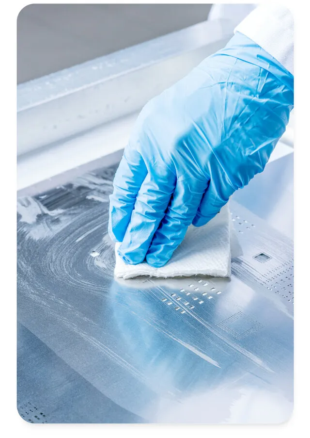
Best practices include dedicated cleaning protocols; nano-coatings tolerate solvent or water-based wipes but benefit from low-residue media to preserve integrity. Reduce wipe frequency by 30 to 50 percent compared to uncoated stencils, focusing on underside only when bridging appears. For troubleshooting poor solder paste transfer efficiency, inspect for coating wear via contact angle measurements; re-coat if below 90 degrees. Pair with optimized stencil tension, typically 20 to 25 Newtons, to maximize gasketing against the PCB.
Incorporate aperture surface treatment into design reviews, using rounded corners or trapezoidal walls to synergize with coatings. Validate via gauge repeat studies, printing 100 cycles and analyzing volume CV under 10 percent. Address common issues like insufficient transfer by increasing print speed slightly or refining paste viscosity. Maintenance logs track coating lifespan, often exceeding 100,000 prints, minimizing unplanned stops.
Troubleshooting Insights for Stencil Performance Issues
Engineers often encounter inconsistent deposits despite solid designs, pointing to stencil condition. If solder paste transfer efficiency drops, check for flux buildup on apertures; nano-coatings delay this, but plasma pre-treatment revives performance. Bridging in dense areas signals excessive volume or poor release, resolvable by finer apertures enabled by coatings. Tombstoning links to uneven paste heights, where coated stencils excel in uniformity.
Volume deficits in small apertures stem from high surface tension; coatings counteract by improving wetting dynamics. Use laser profilometry to quantify wall roughness post-print, targeting sub-micron residues. For reflow defects, correlate SPI data showing CV over 12 percent to recoating needs. These practical diagnostics ensure stencil nano-coatings deliver sustained aperture performance.
Conclusion
Stencil nano-coatings revolutionize SMT stencil performance by optimizing aperture surface treatment and solder paste transfer efficiency. They enable reliable printing for miniaturized assemblies, reducing defects and maintenance. Engineers gain troubleshooting leverage through consistent release and extended usability. Adopting these solutions aligns processes with industry benchmarks, boosting overall assembly quality. As demands intensify, nano-coatings stand as a proven enhancer for high-reliability production.
FAQs
Q1: What is a stencil nano-coating and how does it improve SMT stencil performance?
A1: Stencil nano-coating is an ultra-thin hydrophobic layer applied to aperture walls and stencil surfaces, repelling solder paste flux for cleaner release. It enhances stencil performance by increasing solder paste transfer efficiency, especially in fine-pitch features, and reduces cleaning cycles. This results in uniform deposits and fewer bridging defects during troubleshooting.
Q2: Why is aperture surface treatment critical for solder paste transfer efficiency?
A2: Aperture surface treatment, like nano-coatings, minimizes flux adhesion, promoting complete paste evacuation from stencil walls. Without it, residues cause low transfer volumes and variability, impacting reflow yields. Coatings maintain low surface energy, supporting consistent efficiency across print runs in high-density SMT.
Q3: When should electrical engineers consider nano-coatings for their SMT stencils?
A3: Opt for stencil nano-coatings when designing for low area ratio apertures or components under 0.5 mm pitch, per IPC-7525 guidelines. They excel in high-volume lines with frequent cleaning or paste types prone to sticking. Troubleshooting inconsistent transfer efficiency often resolves with this upgrade.
Q4: How do nano-coatings affect stencil cleaning and maintenance in SMT assembly?
A4: Nano-coatings reduce underside cleaning frequency by repelling residues, extending intervals between wipes. They withstand standard solvents without degradation, preserving aperture performance over thousands of cycles. Regular inspection ensures sustained solder paste transfer efficiency, minimizing downtime.
References
IPC-7525B — Stencil Design Guideline. IPC, 2007
IPC-7527 — Requirements for Solder Paste Printing. IPC, 2015
J-STD-005B — Requirements for Soldering Fluxes. J-STD, 2011


