 ALLPCB


Introduction
Stencil printing represents the foundational step in surface mount technology (SMT) assembly, where precise solder paste deposition determines downstream success. The stencil aperture shape plays a pivotal role in solder paste release, influencing transfer efficiency, deposit volume, and defect rates. Engineers often debate squares versus circles, but specialized forms like home plate apertures offer targeted advantages for challenging components. Understanding these effects helps optimize aperture design for reliable joints. This article explores how shapes impact paste behavior during snap-off, drawing on practical insights for troubleshooting common printing issues. By aligning stencil choices with process needs, teams can enhance yield and minimize rework.
What Is Stencil Aperture Shape and Why It Matters in SMT
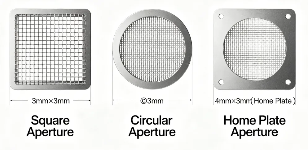
Stencil apertures are the precisely etched openings in a metal foil through which solder paste is forced onto PCB pads during printing. Aperture shape refers to the geometric profile of these openings, such as square, circular, or home plate configurations. In SMT, solder paste release describes the percentage of paste volume that cleanly transfers from the aperture to the pad upon stencil separation. Poor release leads to insufficient deposits, causing open joints or tombstoning, while excess retention results in bridging or solder balls.
Aperture design directly ties to production efficiency, as inconsistent release amplifies defects in high-volume assembly. For electric engineers, selecting the right shape balances volume maximization with clean snap-off, especially for fine-pitch components. Industry guidelines emphasize shape's role alongside factors like stencil thickness and paste rheology. Optimizing this parameter reduces variability in paste in place (PIP) inspections and supports miniaturization trends.
Technical Principles Behind Solder Paste Release
Solder paste release hinges on the interplay between aperture geometry, surface tension, and paste viscosity during the printing cycle's snap-off phase. As the stencil lifts, paste must detach from walls without bridging or residue. Square apertures maximize theoretical volume due to larger area for equivalent dimensions but suffer from corner entrapment, where paste agglomerates and resists release. Circular apertures promote uniform flow and higher transfer efficiency because curved walls minimize stagnation points. Home plate apertures, resembling a trapezoid with a pointed end, leverage laser-cut trapezoidal walls—wider at the board side—to facilitate smoother detachment.
Area ratio, defined as aperture area divided by wall surface area, governs overall releasability; IPC-7525 guidelines recommend values above 0.66 for consistent performance. Thinner stencils (typically 0.1 to 0.127 mm) amplify shape sensitivity, as lower ratios challenge paste flow. For squares, rounded corners mitigate trapping, blending square volume benefits with circular release traits. Home plate designs excel in fine-pitch scenarios by directing paste toward the pad center, reducing peripheral beading.
Paste particle size and flux activity further modulate shape effects; finer Type 4 or 5 pastes pair better with rounded or trapezoidal forms to avoid agglomeration. During filling, squeegee pressure packs paste into apertures, but release dynamics dominate outcomes. Empirical tests reveal squares deposit more volume overall, yet circles and home plates yield lower variation in SPI measurements. Engineers must model these via aspect ratio (minimum dimension over thickness) alongside shape for predictive design.
Related Reading: PCB Stencil Design for Panelization: Achieving Optimal Solder Paste Deposition
Comparing Aperture Shapes: Squares, Circles, and Home Plates
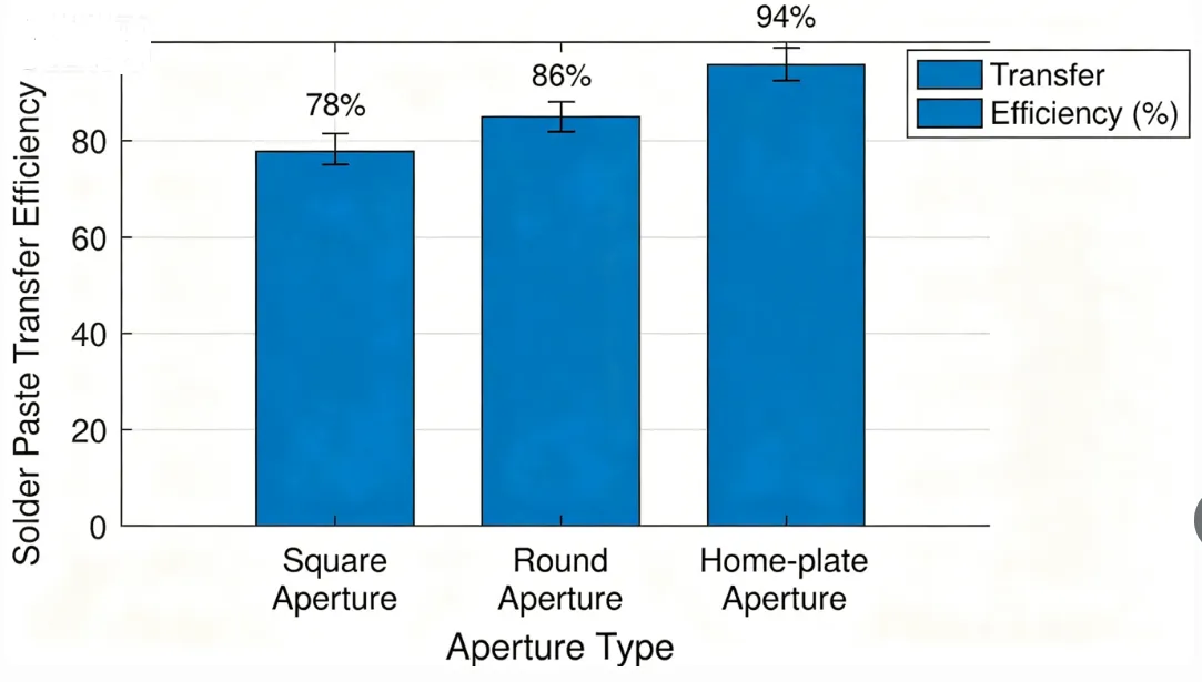
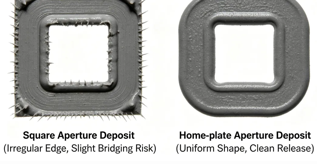
Square apertures suit larger pads where volume trumps release perfection, offering up to 20% more paste than equivalent circles due to edge length advantages. However, sharp 90-degree corners trap paste, leading to inconsistent bricks and higher first-pass defect rates. Troubleshooting tip: If SPI flags low volume on squares, inspect for corner residue and consider radiusing. Circles provide reliable release across pitches, ideal for BGAs, as symmetric curvature ensures even detachment without dead zones.
Home plate apertures address fine-pitch passives like 0201 or 01005, where solder balls plague squares. This trapezoidal shape, often inverted for specific flows, channels paste centrally during release, minimizing satellite formation. Laser etching naturally produces sloped walls in home plates, enhancing demolding compared to electroformed squares. In practice, home plates reduce variability for area ratios near limits, supporting denser boards.
Hybrid "squircle" shapes—squares with rounded corners—emerge as versatile, capturing square volume while approximating circular release. Selection criteria: Use squares for pads over 0.5 mm, circles for uniform QFPs, and home plates for passives under 0.4 mm pitch. Stencil thickness dictates thresholds; 0.125 mm foils favor rounded forms to maintain IPC-7525 area ratios.
Practical Best Practices for Aperture Design in SMT
Start with pad-to-aperture reduction: Shrink openings 5-10% versus land patterns to control bridging, then refine shape based on component type. For squares, apply 0.1-0.2 mm corner radii to boost release without volume loss. Circles work universally but pair with home plates for mixed arrays—test via DOE on coupon panels. Maintain stencil flatness under 25 μm across the frame to ensure uniform gasketing.
Incorporate J-STD-020 handling to prevent paste drying, which exacerbates shape-induced inconsistencies. Print parameters like snap-off distance (0.5-1 mm) and speed (20-50 mm/s) tune release; slower speeds aid home plates on fine features. Post-print SPI verifies >75% PIP uniformity, flagging shape mismatches early. For troubleshooting low release, audit wall finish—electropolishing smooths squares effectively.
Iterate designs in software, simulating area ratios per IPC-7525 before fabrication. Hybrid stencils with zoned shapes optimize diverse boards. Clean stencils every 5-10 prints to preserve aperture integrity, especially sharp-edged squares.
Related Reading: Stencil Aperture Design for Optimal Solder Paste
Troubleshooting Common Issues with Aperture Shapes
Engineers encounter insufficient release most with squares on thin stencils, manifesting as "scooped" deposits. Solution: Switch to home plates or increase radius; verify area ratio exceeds 0.66. Circles may under-volumize large pads, causing cold joints—counter with slight enlargement or squircle transition. Home plates occasionally bead at the point; invert orientation or refine angle for flow.
Solder balls cluster near squares' corners post-reflow—root cause is trapped paste residue. Mitigate via finer powder and polished walls. Bridging spikes with oversized apertures regardless of shape; always reduce versus pads. Process audits reveal 80% of print defects trace to aperture design mismatches.
Conclusion
Stencil aperture shape profoundly influences solder paste release, with squares prioritizing volume, circles ensuring consistency, and home plates tackling fine-pitch challenges. Practical aperture design integrates geometry, ratios, and process controls for optimal SMT outcomes. Adhering to IPC-7525 and J-STD-020 elevates performance, reducing defects and supporting advanced assemblies. Engineers benefit from testing shapes on production-like panels to tailor solutions. Ultimately, informed choices in stencil aperture shape drive reliable, high-yield PCB production.
FAQs
Q1: What is the best stencil aperture shape for solder paste release on fine-pitch components?
A1: Home plate apertures excel for passives under 0.4 mm pitch, as their trapezoidal form directs paste centrally and leverages sloped walls for clean snap-off. This minimizes solder balls compared to squares, which trap residue in corners. Follow IPC-7525 area ratios above 0.66 and test via SPI for validation. Practical troubleshooting involves inverting the home plate if beading persists.
Q2: How does square versus circle aperture design affect SMT transfer efficiency?
A2: Squares maximize paste volume but exhibit slightly lower transfer efficiency due to corner trapping, while circles provide superior release uniformity. For equivalent dimensions, squares deposit more overall paste, suiting larger pads. Blend benefits with radiused squares. Monitor via PIP to adjust for stencil thickness.
Q3: When should I use a home plate aperture in aperture design?
A3: Opt for home plate apertures on small chip components like 01005 to control volume and reduce satellites during solder paste release. Their shape aids flow in low area ratio scenarios. Combine with Type 4/5 paste and polished stencils for best results. Avoid on large pads where volume loss occurs.
Q4: What role do industry standards play in optimizing stencil aperture shape?
A4: Standards like IPC-7525 guide area and aspect ratios for reliable solder paste release across shapes. They ensure designs achieve consistent transfer, preventing defects in SMT. Reference them during DOE to balance square volume with home plate precision.
References
IPC-7525C — Stencil Design Guidelines. IPC, 2021
J-STD-020E — Moisture/Reflow Sensitivity Classification of Nonhermetic Surface Mount Devices. JEDEC/IPC, 2014
IPC-A-610H — Acceptability of Electronic Assemblies. IPC, 2019


