 ALLPCB


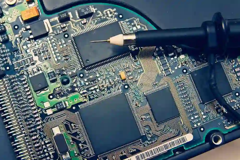
If you're looking to improve the precision and reliability of your surface mount technology (SMT) assembly process, especially for fine-pitch components, optimizing your SMT stencil design is critical. Fine-pitch components, such as 0201 packages and Quad Flat Packages (QFP) with tight lead spacing, demand precise solder paste application to ensure proper connections and avoid defects like bridging or insufficient solder. In this guide, we’ll dive deep into SMT stencil design rules, fine-pitch stencil apertures, solder paste release for fine-pitch, stencil thickness for 0201 components, and aperture reduction for fine-pitch QFP. Whether you're an engineer or a manufacturer, this comprehensive resource will help you achieve better results in your SMT processes.
Why SMT Stencil Design Matters for Fine-Pitch Components
In SMT assembly, the stencil plays a pivotal role by controlling the amount and placement of solder paste on the printed circuit board (PCB). For fine-pitch components—those with lead pitches of 0.5mm or less—any slight error in stencil design can lead to soldering defects. Issues like solder bridging, tombstoning, or insufficient paste can compromise the electrical and mechanical integrity of the assembly. By optimizing stencil design, you ensure consistent solder paste deposition, which directly impacts the quality of the final product.
Key SMT Stencil Design Rules for Precision
To achieve reliable results with fine-pitch components, following established SMT stencil design rules is essential. These guidelines help balance the amount of solder paste deposited while preventing common issues.
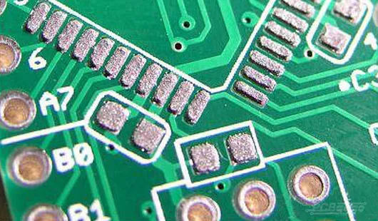
- Aperture-to-Pad Ratio: The aperture size in the stencil should typically be slightly smaller than the PCB pad size to prevent excess paste. A common rule is to aim for an area ratio (aperture area divided by the area of the stencil wall) of at least 0.66 for adequate paste release.
- Stencil Thickness: For fine-pitch components, thinner stencils (typically 0.1mm to 0.12mm) are preferred to control paste volume. Thicker stencils can lead to over-deposition, causing bridging between closely spaced leads.
- Aperture Shape: Rounded corners on apertures reduce the risk of paste clogging and improve release. For fine-pitch designs, trapezoidal apertures (wider at the bottom) can enhance paste transfer efficiency by up to 10-15% compared to straight-walled designs.
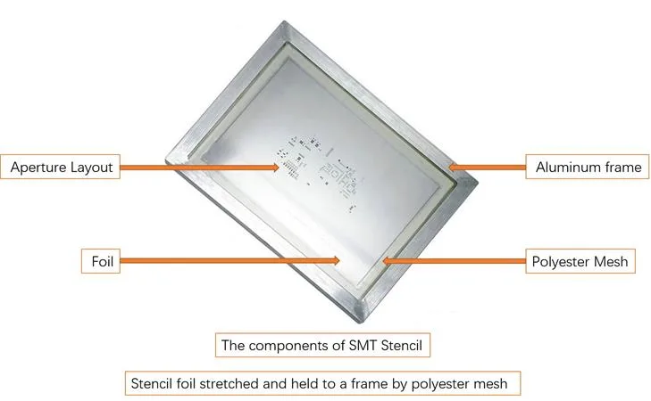
- Material and Finish: Stainless steel stencils with laser-cut apertures and a polished finish ensure smoother paste release, especially for small openings needed in fine-pitch applications.
By adhering to these rules, you can minimize defects and improve the consistency of your SMT process.
Fine-Pitch Stencil Apertures: Balancing Precision and Paste Volume
Designing fine-pitch stencil apertures requires careful consideration of component lead spacing and pad dimensions. Fine-pitch components, such as QFPs with 0.4mm or 0.5mm pitch, have very small pads and tight tolerances. If the aperture is too large, excess paste can cause solder bridges. If it’s too small, insufficient paste can lead to weak joints.
A common practice is to reduce the aperture size by 10-20% compared to the pad size for fine-pitch components. For instance, if a pad measures 0.3mm x 0.6mm, an aperture of 0.27mm x 0.54mm might be ideal. This reduction helps control paste volume while maintaining alignment accuracy during printing.
Additionally, the aspect ratio (aperture width divided by stencil thickness) should be at least 1.5 to ensure proper paste release. For a 0.1mm thick stencil, the smallest aperture width should be no less than 0.15mm. For ultra-fine-pitch components, advanced techniques like electroformed stencils can achieve even smaller apertures with higher precision.
Solder Paste Release for Fine-Pitch: Challenges and Solutions
Ensuring effective solder paste release for fine-pitch components is one of the biggest challenges in SMT stencil design. With smaller apertures, the solder paste is more likely to stick to the stencil walls rather than transfer to the PCB pads. This can result in incomplete deposits and inconsistent soldering.
To improve paste release, consider the following strategies:
- Optimize Area Ratio: As mentioned earlier, maintain an area ratio above 0.66. For very small apertures, reducing stencil thickness can help achieve this ratio. For example, for a 0.2mm x 0.2mm aperture, a 0.1mm thick stencil yields an area ratio of 0.8, which supports good release.
- Use Nano-Coatings: Applying a nano-coating to the stencil surface can reduce friction and improve paste release by up to 20%, especially for fine-pitch applications.
- Adjust Printing Parameters: Slower squeegee speeds (around 20-40mm/s) and higher pressure can help push paste through small apertures more effectively.
Testing and iterating on these parameters during the prototyping phase can significantly reduce defects in production runs.
Stencil Thickness for 0201 Components: Finding the Right Balance
When working with ultra-small components like 0201 packages (measuring just 0.6mm x 0.3mm), selecting the correct stencil thickness for 0201 components is critical. These tiny components require minimal solder paste to avoid bridging, yet enough to form a reliable joint.
A stencil thickness of 0.08mm to 0.1mm is typically recommended for 0201 components. This range allows for an aperture size of approximately 0.25mm x 0.25mm, delivering a controlled paste volume of about 0.0015 to 0.002 cubic millimeters per pad. If the stencil is too thick (e.g., 0.15mm), the paste volume can increase by 50% or more, raising the risk of defects.
For mixed assemblies with both 0201 and larger components, a step stencil can be used. This design features thinner areas (e.g., 0.08mm) for fine-pitch zones and thicker areas (e.g., 0.12mm) for standard components, ensuring optimal paste deposition across the board.
Aperture Reduction for Fine-Pitch QFP: Precision in Tight Spaces
Quad Flat Packages (QFP) with fine-pitch leads (0.5mm or less) require specific attention to aperture reduction for fine-pitch QFP. The goal is to deposit just enough solder paste to form a strong joint without causing bridging between adjacent leads.
For QFP components, a common approach is to reduce the aperture width by 10-15% compared to the pad width while maintaining the full length of the pad. For example, for a pad measuring 0.3mm wide by 1.2mm long, the aperture might be reduced to 0.25mm wide by 1.2mm long. This reduction minimizes the risk of excess paste while ensuring coverage along the entire pad for a reliable connection.
Additionally, consider spacing between apertures. For 0.5mm pitch QFP, the stencil should maintain at least 0.2mm of separation between adjacent apertures to prevent paste from merging during printing. Laser-cut stencils with high precision are often necessary to achieve these tight tolerances.
Advanced Techniques for SMT Stencil Optimization
Beyond the basics, several advanced techniques can further enhance stencil performance for fine-pitch components:
- Electroformed Stencils: These stencils offer superior precision for ultra-fine apertures (below 0.15mm), with smoother walls that improve paste release by up to 25% compared to traditional laser-cut stencils.
- Step Stencils: As mentioned earlier, step stencils accommodate mixed component sizes on a single board, allowing for tailored paste volumes in different areas.
- 3D Stencil Printing: For complex designs, 3D stencil printing technology can create multi-level apertures, providing even greater control over paste deposition.
Implementing these techniques may increase initial costs but can significantly reduce defects and rework in high-volume production.
Common Pitfalls to Avoid in SMT Stencil Design
Even with the best intentions, mistakes in stencil design can lead to costly issues. Here are some pitfalls to watch out for:
- Overlooking Area Ratio: Failing to calculate and maintain an adequate area ratio can result in poor paste release, especially for fine-pitch components.
- Inconsistent Stencil Thickness: Using a uniform thickness for mixed assemblies can lead to over- or under-deposition of paste, depending on component size.
- Ignoring Environmental Factors: Temperature and humidity in the assembly environment can affect solder paste viscosity and release. Ensure your stencil design accounts for these variables by testing under real-world conditions.
Regular inspection and maintenance of stencils, such as cleaning after every 5-10 prints, can also prevent buildup and ensure consistent performance.
How to Test and Validate Your Stencil Design
Before moving to full-scale production, validating your stencil design is a must. Use these steps to ensure optimal performance:
- Prototype Testing: Print a small batch of boards using the stencil and inspect the paste deposits under a microscope. Look for uniformity and check for bridging or insufficient paste.
- Solder Joint Analysis: After reflow, examine the solder joints for defects. Use X-ray inspection for hidden joints like those under BGA packages.
- Iterate Based on Results: Adjust aperture sizes, stencil thickness, or printing parameters based on test outcomes. Repeat the process until defects are minimized.
Investing time in validation can save significant costs by preventing issues in high-volume runs.
Conclusion: Mastering SMT Stencil Design for Fine-Pitch Success
Optimizing SMT stencil design for fine-pitch components is a complex but essential task for achieving high-quality PCB assemblies. By following SMT stencil design rules, fine-tuning fine-pitch stencil apertures, ensuring effective solder paste release for fine-pitch, selecting the right stencil thickness for 0201 components, and applying aperture reduction for fine-pitch QFP, you can significantly improve the reliability and performance of your products.
At ALLPCB, we understand the challenges of SMT assembly and are committed to supporting engineers and manufacturers with high-quality stencil solutions tailored to your specific needs. Whether you're working on ultra-small 0201 components or intricate QFP designs, mastering stencil optimization is the key to success in modern electronics manufacturing.


