 ALLPCB


Introduction
Surface mount technology (SMT) assembly relies heavily on precise solder paste application during the printing process. The stencil serves as the critical interface that transfers solder paste onto PCB pads, and its aperture design directly influences the quality of deposits. Poor aperture design leads to common defects such as bridging, tombstoning, and insufficient solder paste release, which reduce yields and increase rework costs. Engineers must master SMT stencil aperture size, aperture shape, and related parameters to achieve reliable assembly. This article explores stencil design rules that minimize these issues while optimizing production efficiency. By focusing on practical engineering principles, designers can enhance first-pass yields in high-volume manufacturing.
Understanding SMT Stencil Apertures and Their Role
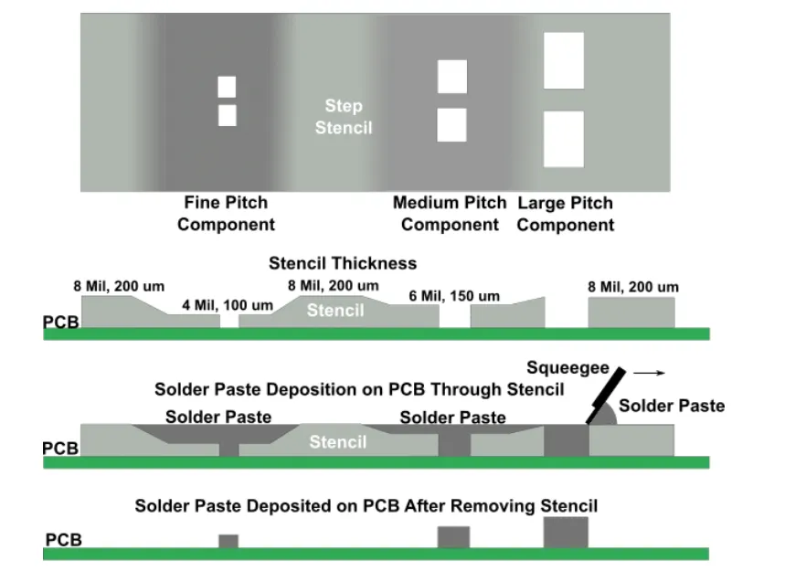
Stencil apertures are precisely etched openings in the thin metal foil that align with PCB pads to deposit solder paste. Each aperture's dimensions determine the volume and shape of the paste brick transferred during printing. Factors like stencil thickness, typically ranging from fine-pitch requirements to standard thicknesses, interact with aperture geometry to affect paste release. In SMT processes, consistent paste volume ensures proper joint formation during reflow. Aperture misalignment or suboptimal design causes variations in deposit height and width, leading to assembly failures. Mastering these elements is essential for electric engineers tackling complex boards with mixed component sizes.
The relevance of aperture design intensifies with shrinking component pitches, such as 0.3mm or finer. As pads become smaller, the margin for error decreases, amplifying the impact of minor design flaws. Defects like bridging occur when excess paste spans adjacent pads, while tombstoning happens due to uneven reflow forces from imbalanced paste volumes. Solder paste release efficiency drops if apertures trap paste on walls rather than releasing it cleanly. Industry guidelines emphasize calculating key ratios early in the design phase to predict performance. This proactive approach aligns with quality control in PCB assembly lines.
Key Technical Principles of Aperture Design
SMT stencil aperture size should generally match the pad dimensions but with a slight reduction to prevent paste bridging. Common practice reduces aperture width by a small margin relative to the pad, ensuring paste stays centered during printing. This adjustment accounts for paste flow and squeegee pressure, promoting uniform deposits. For fine-pitch components, even minor oversizing leads to defects, so precision laser etching becomes crucial. Engineers calculate sizes based on component datasheets and pad layouts to maintain volume consistency. Aperture size directly ties into solder paste release, where undersized openings risk starvation, and oversized ones promote slumping.
Aperture shape significantly influences paste transfer efficiency and defect rates. Rectangular apertures suit most QFP and SOIC leads but can cause bridging at corners due to paste buildup. Trapezoidal shapes, narrower at the bottom, facilitate clean release by reducing wall adhesion. Rounded or squircle ends minimize first-bridge defects by smoothing paste flow. For thermal pads on QFN or BGA, window-pane patterns divide large areas into smaller apertures, improving release and reducing voids. Shape selection depends on pitch and paste type, with testing validating choices in production.
Central to stencil design rules are the aspect ratio and area ratio, as defined in IPC-7525. The aspect ratio, aperture width divided by stencil thickness, should exceed 1.5 to ensure walls do not dominate paste release. Below this threshold, paste clings to vertical walls, causing incomplete transfers. The area ratio, aperture opening area divided by wall surface area, targets above 0.66 for reliable deposition across shapes. These metrics predict printability before fabrication, guiding thickness choices like 100 microns for fine pitch. IPC-7525 provides the framework for these calculations, helping engineers avoid empirical trial-and-error.
Related Reading: Advanced Stencil Aperture Designs for Optimized Solder Paste Deposition
Practical Best Practices for Aperture Optimization
Start with standard stencil thicknesses and adjust based on smallest pitch. For pitches under 0.5mm, thinner stencils improve ratios but require robust frames. Combine this with aperture reductions of 5-10% on pad size for peripheral leads, balancing volume and bridging risk. Verify designs using simulation software that models paste rheology under print conditions. Iterate with trial prints on scrap panels to measure transfer efficiency empirically. These steps ensure stencil design rules translate to high yields.
To minimize bridging, incorporate rounded corners with radii at least 25% of aperture width. Trapezoidal apertures with 10-15 degree tapers aid demolding, reducing sidewall tension. For dense arrays, maintain pitch-to-aperture gaps at least equal to stencil thickness. Home plating on apertures enhances release for ratios near limits. Adjust squeegee speed and pressure post-design, but prioritize geometry fixes first. Consistent application across board zones prevents zone-specific bridging.
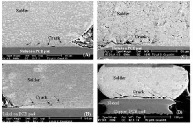
Tombstoning, prevalent in chip components like 0402, stems from asymmetric paste volumes causing uneven reflow wetting. Reduce paste on the larger pad end by 10-20% via shortened or U-shaped apertures. This equalizes pull forces during melting. For paired pads, ensure symmetrical designs relative to component center. J-STD-001 guidelines for solder joints reinforce balancing volumes to avoid lift-off. Troubleshooting involves reflow profiling alongside stencil tweaks for root-cause resolution.
Related Reading: Stencil Aperture Design for Optimal Solder Paste
For fine-pitch BGA or LGA, segment large apertures into grids matching ball pitch. This maintains area ratios while controlling total volume. Type 4 or finer paste pairs best with high ratios. Electroformed stencils offer smoother walls for challenging geometries. Validate with AOI post-print to quantify defects before reflow commitment.
Troubleshooting Common Defects Through Aperture Adjustments
Bridging often traces to square-ended rectangles or excessive volumes. Switch to oblong or home-plated trapezoids, and reduce aperture length by 0.1mm per end. Check gaps between apertures; minimums prevent paste bridging during snap-off. If reflow bridging persists, it signals volume overload, addressed by 75% transfer targets.
Insufficient solder paste release appears as skips or low deposits. Calculate area ratios first; below 0.66 demands thinner stencils or electroforming. Polish apertures post-etch for nano-coatings if needed. Uneven release across boards points to warpage; flatness checks precede printing.
Tombstoning requires pad-specific tweaks. For non-square chips, elongate the toe-side aperture slightly while reducing heel volume. This promotes simultaneous wetting. Monitor with SPI for volume uniformity pre-reflow.
Conclusion
Effective SMT stencil aperture design hinges on precise control of size, shape, aperture ratio, and area ratio. Adhering to IPC-7525 principles ensures solder paste release exceeds 75-80% consistently, slashing defects like bridging and tombstoning. Practical troubleshooting integrates ratios with shape optimizations for real-world yields. Electric engineers benefit from early ratio calculations and iterative validation. Implementing these stencil design rules elevates assembly reliability across production scales.
FAQs
Q1: What is the ideal SMT stencil aperture size relative to PCB pads?
A1: Aperture size should be slightly smaller than the pad, often by 5-10%, to center paste and avoid bridging. This rule applies especially to fine-pitch components where excess paste causes slumping. Calculate based on pad geometry and verify with print trials for optimal solder paste release. Stencil design rules prevent off-pad deposition while maintaining joint volume.
Q2: How does aperture shape affect bridging in SMT assembly?
A2: Rectangular shapes with sharp corners promote paste buildup, leading to bridging. Trapezoidal or rounded ends smooth flow, reducing first-print bridges. For dense areas, squircle approximations enhance release. Pair with adequate gaps to minimize defects per stencil design rules.
Q3: What role does area ratio play in solder paste release?
A3: Area ratio, per IPC-7525, measures opening area against wall area; above 0.66 ensures clean release. Low ratios trap paste, causing skips. Thinner stencils boost ratios for fine apertures. Engineers use this metric to predict printability.
Q4: How can stencil design rules prevent tombstoning?
A4: Balance paste volumes on chip ends with reduced heel-side apertures or U-shapes. This equalizes reflow forces, avoiding lift-off. Symmetrical designs for square pads suffice, but asymmetry demands tweaks. Validate with SPI for uniformity.
References
IPC-7525B — Stencil Design Guidelines. IPC, 2011
IPC-7525C — Stencil Design Guidelines. IPC, 2018
J-STD-001H — Requirements for Soldered Electrical and Electronic Assemblies. IPC, 2020


