ALLPCB


Introduction
Lead-free assembly processes higher soldering temperatures compared to traditional tin-lead solders, placing greater demands on PCB laminates. Engineers must select materials that withstand repeated thermal excursions without compromising structural integrity or electrical performance. Poor laminate choice can result in issues such as delamination, warpage, or via cracking during reflow soldering. This guide examines key properties and selection criteria for high Tg laminate lead-free PCB applications. By focusing on material behaviors under elevated temperatures, designers can ensure reliable assembly outcomes. Understanding these factors aligns with industry requirements for robust electronics manufacturing.
Why Lead-Free Assembly Challenges Traditional Laminates
Lead-free solders require peak reflow temperatures substantially higher than those for leaded alloys, accelerating material degradation in standard laminates. Conventional FR-4 materials with lower glass transition temperatures soften during these profiles, leading to dimensional instability. This shift became necessary due to environmental regulations restricting hazardous substances, compelling the industry to adapt PCB materials accordingly. Mismatched thermal expansion between laminate and copper layers exacerbates stresses, potentially causing board warpage or solder joint failures post-assembly. Engineers face the task of balancing cost, performance, and process compatibility when upgrading to lead-free compatible laminates. The consequences of inadequate selection manifest in reduced assembly yields and long-term reliability concerns.
Related Reading: RoHS Compliance for Beginners: A Simple Guide to Lead Free Assembly
Key Material Properties for Lead-Free PCB Performance
Lead-free PCB material properties center on thermal stability, mechanical strength, and dimensional control during high-temperature exposure. Glass transition temperature, or Tg, marks the point where the resin transitions from glassy to rubbery state, critical for maintaining rigidity through multiple reflow cycles. High Tg laminates resist softening, preserving via integrity and surface planarity. Coefficient of thermal expansion, or CTE, influences stress distribution across layers, with mismatches between copper foil and laminate core promoting cracks in plated through-holes. Decomposition temperature, Td, indicates resistance to thermal breakdown, ensuring no outgassing or charring occurs. These properties collectively define lead-free PCB thermal performance, guiding material qualification.
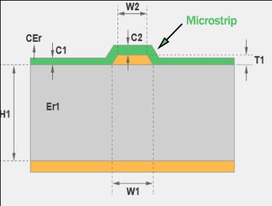
Lead-free PCB CTE becomes particularly relevant in multilayer boards where copper planes and dielectric layers interact under thermal cycling. Laminates engineered for low CTE in the Z-axis minimize barrel cracking in vias subjected to reflow stresses. Electrical properties such as dielectric constant and loss tangent remain stable in high Tg materials, supporting signal integrity in dense designs. Moisture absorption affects these behaviors, as absorbed water vaporizes explosively during reflow, potentially causing delamination. Standards like IPC-4101 outline qualification tests for these properties, ensuring consistency across suppliers. Selecting laminates based on verified data prevents field failures in demanding applications.
The Role of High Tg Laminates in Lead-Free Assembly
High Tg laminate lead-free PCB designs address the primary challenge of elevated reflow temperatures by providing superior heat resistance. These materials maintain mechanical modulus above typical peak soldering conditions, reducing the risk of board sag or component shift during processing. In contrast to standard Tg materials, high Tg variants exhibit minimal viscosity increase, supporting precise solder paste melting and wetting. This property proves essential for assemblies involving fine-pitch components or bottom-side reflow after top-side population. Reliability improves as high Tg laminates endure subsequent processes like conformal coating or rework without property degradation. Engineers specify these for applications expecting harsh thermal environments or multiple assembly steps.
Beyond Tg, high Tg laminates often incorporate fillers to optimize CTE alignment with copper, enhancing overall board stability. During cooling from reflow, controlled contraction prevents micro-cracks at copper-dielectric interfaces. Z-axis expansion control proves vital for thick multilayer stacks, where cumulative stresses amplify failure risks. Thermal performance extends to time-to-delamination metrics, indicating endurance under prolonged heat. J-STD-020 defines reflow conditions that test these capabilities, classifying materials for moisture sensitivity alongside thermal robustness. Integrating high Tg materials elevates lead-free PCB thermal performance to meet evolving assembly demands.
Related Reading: Material Selection Secrets: Choosing the Right Laminates for High Performance Missile Guidance PCBs
Criteria for Lead-Free PCB Laminate Selection
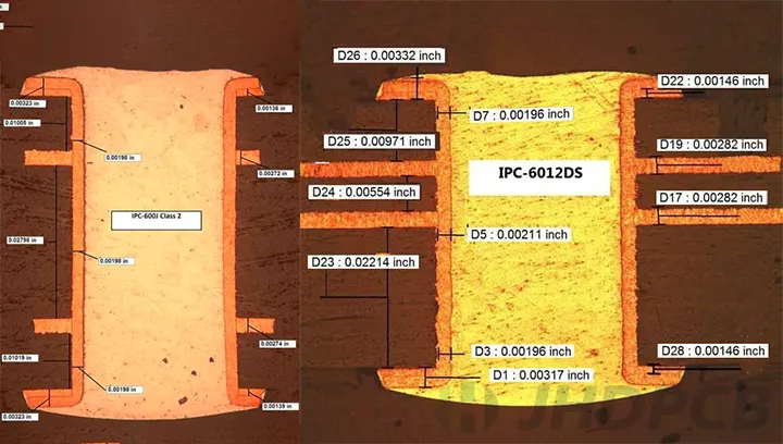
Lead-free PCB laminate selection hinges on matching material properties to specific assembly profiles and end-use conditions. Begin by evaluating Tg requirements against anticipated peak temperatures and reflow cycle counts, favoring materials exceeding standard FR-4 thresholds. Assess CTE values across X, Y, and Z directions to ensure compatibility with copper foil and component leads, minimizing warpage in asymmetric stacks. Td and T260/T288 ratings predict resistance to charring and delamination during soldering. Consider layer count and copper weight, as thicker constructions demand enhanced mechanical support. Fabricators reference IPC-6012 for performance verification post-lamination.
Additional factors include dielectric thickness uniformity and peel strength, which influence impedance control and trace adhesion under thermal stress. For high-reliability sectors, prioritize low-halogen or halogen-free options to mitigate corrosion risks in humid environments. Simulate thermal profiles early in design to validate laminate choices, correlating simulations with material datasheets. Cost-benefit analysis weighs premium high Tg materials against failure mitigation value. Procurement specifications should invoke slash sheets from IPC-4101 to guarantee lead-free compatibility. This systematic approach optimizes lead-free PCB laminate selection for production scalability.
Best Practices for Implementing High Tg Laminates
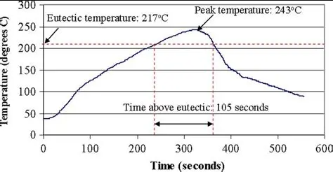
Specify high Tg laminates explicitly in fabrication drawings, referencing applicable IPC-4101 slash sheets for unambiguous supplier qualification. Conduct design reviews incorporating thermal modeling to predict warpage based on CTE differentials and board geometry. Optimize reflow profiles per J-STD-020 guidelines, ramping slowly to avoid shocking laminates with rapid heating. Bake boards prior to assembly if moisture sensitivity exceeds level 3, preventing popcorn effects during soldering. Implement post-reflow inspections for warpage and delamination using shadow moiré or dial gauge methods. These practices ensure consistent lead-free PCB thermal performance across production runs.
Layer stackup symmetry aids in warpage control, pairing high Tg cores with compatible prepregs for uniform CTE. Select copper foils with reverse-treated surfaces for better adhesion in high Tg systems. Validate assemblies through accelerated thermal cycling to confirm long-term stability. Collaborate with fabricators on material traceability, verifying Td and Tg via differential scanning calorimetry if needed. Document process windows to refine future builds, reducing variability. Adhering to these steps minimizes defects in high Tg laminate lead-free PCB manufacturing.
Conclusion
Selecting the appropriate PCB laminate for lead-free assembly demands attention to Tg, CTE, and thermal stability to counter elevated reflow stresses. High Tg laminates provide the necessary robustness, ensuring dimensional control and reliability in modern electronics. By prioritizing lead-free PCB material properties and adhering to established standards, engineers achieve higher yields and durable products. Practical selection criteria and best practices further mitigate risks associated with thermal mismatch and degradation. Ultimately, informed choices enhance lead-free PCB thermal performance across diverse applications. This approach supports sustainable manufacturing without sacrificing quality.
FAQs
Q1: What makes high Tg laminate essential for lead-free PCB assembly?
A1: High Tg laminates maintain rigidity during the higher peak temperatures of lead-free reflow profiles, preventing softening that leads to warpage or via failures. They offer superior lead-free PCB thermal performance by resisting dimensional changes above standard FR-4 limits. Engineers select them for multilayer boards or repeated soldering cycles to ensure mechanical integrity. This property aligns with IPC-4101 specifications for base materials.
Q2: How does lead-free PCB CTE impact assembly reliability?
A2: CTE mismatch between laminate and copper generates stresses during heating and cooling, risking cracks in plated holes or board bow. Low-CTE high Tg materials minimize this in Z-axis expansion, supporting stable solder joints. Proper selection improves lead-free PCB laminate selection outcomes, especially in thick stacks. Thermal cycling tests verify performance under operational loads.
Q3: What role does J-STD-020 play in lead-free PCB laminate selection?
A3: J-STD-020 outlines moisture/reflow sensitivity classifications and profiles for lead-free processes, guiding laminate thermal endurance evaluation. It ensures materials withstand peak temperatures without delamination. Engineers use it alongside material datasheets for high Tg laminate lead-free PCB validation. Compliance reduces assembly defects from vapor pressure.
Q4: How to evaluate lead-free PCB material properties for a design?
A4: Review Tg, CTE, Td, and delamination times from supplier data against reflow requirements. Simulate stackups for warpage prediction using CTE values. Qualify via IPC-6012 performance specs for qualification. This structured assessment optimizes lead-free PCB thermal performance.
References
IPC-4101E — Specification for Base Materials for Rigid and Multilayer Printed Boards. IPC, 2017
IPC-6012E — Qualification and Performance Specification for Rigid Printed Boards. IPC, 2017
JEDEC J-STD-020E — Moisture/Reflow Sensitivity Classification. JEDEC, 2014