ALLPCB


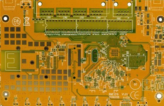
In the rapidly growing world of Internet of Things (IoT), designing efficient and compact printed circuit boards (PCBs) is crucial. A single-layer PCB for IoT offers a cost-effective and space-saving solution for small, low-power devices like sensors and wearable gadgets. But how do you optimize a single-layer PCB for low power and small size without compromising performance? This blog dives deep into the essentials of low power PCB design, compact PCB antenna integration, and single-sided PCB for sensors, providing actionable tips to create efficient IoT device PCB layouts.
Whether you're an engineer or a hobbyist, this guide will walk you through the key considerations and techniques to design a single-layer PCB that meets the unique demands of IoT applications. Let’s explore the process step by step, from understanding the basics to advanced optimization strategies.
Why Choose Single-Layer PCB for IoT Applications?
Single-layer PCBs, also known as single-sided PCBs, consist of a single conductive layer on one side of a non-conductive substrate. This simplicity makes them an ideal choice for IoT devices where cost, size, and power efficiency are top priorities. Here’s why they stand out:
- Cost-Effective: With only one layer of copper, manufacturing costs are significantly lower compared to multi-layer boards.
- Compact Design: They are perfect for small IoT devices like sensors and trackers that require minimal space.
- Simplified Assembly: Components are placed on one side, making assembly and soldering easier, especially for low-complexity circuits.
- Low Power Suitability: Many IoT devices operate on battery power, and single-layer PCBs can be optimized to minimize power consumption.
For IoT applications, where devices often need to be small and energy-efficient, a well-designed single-layer PCB for IoT can deliver reliable performance without unnecessary complexity.
Key Challenges in Single-Layer PCB Design for IoT
While single-layer PCBs offer many benefits, designing them for IoT comes with specific challenges. Addressing these early in the design process ensures better performance and reliability.
1. Limited Routing Space
With only one conductive layer, routing traces for multiple components can become tricky. Overcrowded traces can lead to signal interference and increased resistance, impacting the device’s efficiency.
2. Power Consumption Constraints
IoT devices often run on small batteries, requiring low power PCB design techniques to extend battery life. Poor layout choices can result in unnecessary power loss through heat dissipation or inefficient current paths.
3. Antenna Integration
Many IoT devices rely on wireless communication, necessitating a compact PCB antenna. Fitting an effective antenna on a small single-layer board while avoiding interference is a common hurdle.
4. Component Placement for Sensors
Designing a single-sided PCB for sensors requires careful placement to avoid noise and ensure accurate data collection. Sensors are sensitive to electromagnetic interference (EMI), which can be hard to manage on a single layer.
Understanding these challenges helps in crafting an IoT device PCB layout that balances size, power, and performance.
Best Practices for Single-Layer PCB Design in IoT
Creating an optimized single-layer PCB for IoT involves strategic planning and attention to detail. Below are proven techniques to achieve low power consumption and small size while maintaining functionality.
1. Prioritize Component Placement
Start by placing critical components like microcontrollers, sensors, and power regulators in a logical order. Group related components together to minimize trace lengths. For example, place a temperature sensor close to its analog-to-digital converter to reduce noise in the signal path.
Keep high-current components away from sensitive analog parts to avoid interference. If space allows, dedicate a small area for power components and another for signal processing to improve clarity in your IoT device PCB layout.
2. Optimize Trace Routing
Since single-layer PCBs lack additional layers for routing, trace design is critical. Use wider traces for power lines to handle higher currents with minimal resistance. For instance, a power trace carrying 500mA should ideally be at least 20 mils wide to prevent overheating, assuming a standard 1 oz copper thickness.
For signal traces, keep them as short and direct as possible to reduce signal delay and interference. Avoid crossing traces by using jumpers if necessary, though this should be a last resort as it adds complexity.
3. Focus on Low Power PCB Design Techniques
IoT devices often need to operate for months or years on a single battery. Here are specific low power PCB design strategies:
- Use Low-Power Components: Choose microcontrollers with sleep modes that consume less than 1μA in standby, such as certain ARM Cortex-M0+ chips.
- Minimize Leakage Currents: Avoid long traces near power lines that could cause parasitic capacitance, leading to leakage. Keep power traces short and insulated.
- Decoupling Capacitors: Place 0.1μF capacitors near power pins of ICs to stabilize voltage and reduce noise, which can otherwise increase power draw.
By implementing these techniques, you can significantly extend the battery life of your IoT device.
4. Integrate a Compact PCB Antenna
Wireless communication is a cornerstone of IoT, and embedding a compact PCB antenna directly on the board saves space and cost. Common antenna types for single-layer designs include inverted-F antennas (IFA) and meandered line antennas, which are suitable for frequencies like 2.4 GHz (used in Bluetooth and Wi-Fi).
Design the antenna in a clear area of the PCB, away from ground planes and other components, to minimize interference. For a 2.4 GHz IFA, the antenna length should be approximately 31mm (a quarter wavelength) to achieve optimal resonance. Use simulation tools to fine-tune the impedance matching, aiming for a 50-ohm match to maximize power transfer.
Keep in mind that the PCB material and thickness affect antenna performance. A standard FR-4 substrate with a dielectric constant of 4.4 works well for most IoT frequencies below 6 GHz, as noted in industry resources.
5. Design for Single-Sided PCB Sensors
When designing a single-sided PCB for sensors, noise reduction is paramount. Sensors like accelerometers or humidity sensors can pick up EMI from nearby traces or components. Place sensors at the edge of the board if possible, away from high-frequency digital signals.
Use a small ground pour under the sensor if space allows, even on a single-layer board, to act as a shield. Connect this pour to the main ground with a single point to avoid ground loops. For analog sensors, route their traces away from digital lines to prevent crosstalk.
Advanced Tips for IoT Device PCB Layout
Beyond the basics, there are advanced strategies to further optimize your IoT device PCB layout for performance and efficiency on a single-layer board.
1. Thermal Management
Even low-power IoT devices generate heat, which can affect performance if not managed. Place heat-generating components like voltage regulators near the board’s edge for better dissipation. If using a small heatsink, ensure it doesn’t interfere with other components.
For a component dissipating 0.5W, ensure at least 100mm2 of copper area around it to act as a heat spreader, assuming a 1 oz copper layer. This helps keep temperatures within safe limits, typically below 85°C for most IoT components.
2. EMI Mitigation
Electromagnetic interference can degrade the performance of wireless IoT devices. Since single-layer PCBs lack dedicated ground planes, use strategic trace spacing to minimize EMI. Keep a minimum spacing of 3 times the trace width between high-speed signal traces to reduce coupling.
If your design includes a compact PCB antenna, ensure no traces or components are within 5mm of the antenna area to avoid detuning or interference.
3. Test Points for Debugging
Add small test points to critical nodes like power supply lines and sensor outputs. These allow easy access for debugging without adding bulk to the board. Label them clearly in your design files for future reference.
Tools and Resources for Single-Layer PCB Design
Designing a single-layer PCB for IoT doesn’t require expensive tools. Many free and open-source software options offer robust features for layout and simulation. Look for tools that support antenna design and power analysis to ensure your board meets low-power and small-size goals.
Additionally, leverage online calculators for trace width and antenna length to match your specific current and frequency requirements. For instance, a trace width calculator can confirm that a 10-mil trace is sufficient for a 100mA signal line with minimal voltage drop.
Conclusion: Building Efficient IoT Devices with Single-Layer PCBs
Designing a single-layer PCB for IoT is a balancing act between size, power, and performance. By focusing on low power PCB design, integrating a compact PCB antenna, and optimizing layouts for single-sided PCB for sensors, you can create efficient and reliable IoT devices. Thoughtful component placement, trace routing, and noise management are key to overcoming the limitations of single-layer boards.
With the strategies outlined in this guide, you’re equipped to tackle the challenges of IoT device PCB layout and build compact, power-efficient solutions. Start small, test often, and iterate on your designs to achieve the best results for your IoT projects.