ALLPCB


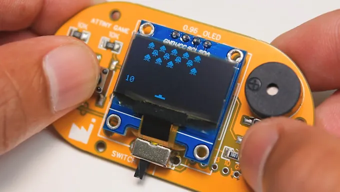
In the fast-evolving world of portable gaming devices, creating smaller, lighter, and more powerful systems is a top priority. The key to achieving this lies in the miniaturization of printed circuit boards (PCBs). But how do designers tackle the challenge of shrinking PCBs while maintaining performance for gaming applications? This guide dives deep into miniaturization techniques for portable gaming device PCBs, covering high-density PCB layout for gaming, compact PCB design challenges, component selection for small PCBs, microvia technology in gaming applications, and HDI PCB design considerations for gaming. Whether you're an engineer or a designer, this comprehensive resource will help you navigate the complexities of compact PCB design with practical insights and actionable strategies.
Why Miniaturization Matters in Portable Gaming Devices
Portable gaming devices, such as handheld consoles and mobile gaming systems, demand a perfect balance of performance, power efficiency, and size. Miniaturization of PCBs plays a critical role in meeting these needs. Smaller PCBs allow for slimmer, more ergonomic designs, while also enabling the integration of advanced features like high-resolution displays, faster processors, and longer battery life. However, shrinking a PCB without compromising functionality is no easy task. It requires careful planning, innovative techniques, and a deep understanding of high-density layouts tailored for gaming applications.
Key Miniaturization Techniques for Gaming Device PCBs
Let’s explore the core techniques that enable the creation of compact, high-performance PCBs for portable gaming devices. These methods focus on optimizing space, enhancing signal integrity, and ensuring thermal management in tight layouts.
1. High-Density PCB Layout for Gaming
A high-density PCB layout is essential for gaming devices where space is limited, but performance cannot be sacrificed. High-density interconnect (HDI) technology allows designers to pack more components into a smaller area by using finer traces and smaller vias. For gaming applications, this means fitting powerful GPUs, CPUs, and memory chips onto a compact board without signal loss or interference.
In practice, high-density PCB layouts for gaming often involve trace widths as small as 3 mils (0.003 inches) and spacing of 3 mils or less. This precision reduces the board's footprint while maintaining signal speeds critical for real-time gaming performance, often exceeding 1 GHz for modern processors. However, such tight layouts require advanced design software and manufacturing processes to ensure accuracy and reliability.
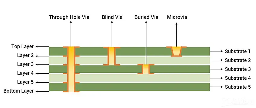
2. Leveraging Microvia Technology in Gaming Applications
Microvia technology is a game-changer for miniaturization in gaming PCBs. Microvias are tiny holes, typically less than 6 mils (0.006 inches) in diameter, that connect different layers of a PCB. Unlike traditional through-hole vias, microvias take up less space and allow for higher routing density. In gaming applications, where multilayer boards are common to handle complex circuitry, microvias enable designers to create intricate connections without increasing the board size.
For example, a portable gaming device might use a 6-layer PCB with microvias to route signals between layers efficiently. This not only saves space but also improves signal integrity by reducing parasitic capacitance and inductance, ensuring smooth gameplay even at high frequencies. Microvia technology in gaming applications is often paired with HDI designs to maximize compactness and performance.
3. HDI PCB Design Considerations for Gaming
HDI PCB design is a cornerstone of miniaturization for portable gaming devices. Beyond just using microvias, HDI design involves several considerations to ensure the board meets the demands of gaming hardware. These include layer stacking, impedance control, and power distribution.
In gaming devices, where components like high-speed processors and graphics chips generate significant heat and require stable power, HDI PCBs often use a stacked via structure. This involves placing microvias on top of each other to connect multiple layers, reducing the board's overall thickness. Impedance control is another critical factor, with designers targeting specific values (e.g., 50 ohms for high-speed signals) to prevent signal reflection and ensure data integrity during intense gaming sessions.
Additionally, power distribution networks in HDI PCBs for gaming must be carefully planned to minimize voltage drops and noise. This often means embedding power and ground planes within the board's inner layers, a technique that saves space while enhancing electrical performance.
Compact PCB Design Challenges and Solutions
While miniaturization offers clear benefits, it also introduces several challenges in compact PCB design for gaming devices. Let’s break down the most common hurdles and how to overcome them.
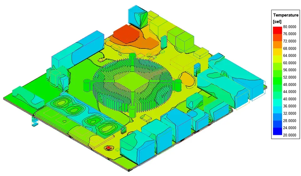
1. Thermal Management in Tight Spaces
Portable gaming devices generate significant heat due to powerful components packed into a small area. Without proper thermal management, this heat can degrade performance or damage the device. In compact PCB designs, traditional heat sinks may not fit, so designers often rely on thermal vias and copper pours to dissipate heat. For instance, placing thermal vias near high-power components can transfer heat to a ground plane or external layer, keeping temperatures in check.
Another solution is using materials with high thermal conductivity, such as metal-core PCBs, though these must be balanced with cost considerations. Simulations during the design phase can also predict hotspots, allowing for strategic component placement to avoid thermal buildup.
2. Signal Integrity at High Frequencies
Gaming devices rely on high-speed signals for seamless graphics and responsiveness. However, compact PCB layouts with tightly packed traces can lead to crosstalk and electromagnetic interference (EMI). To address this, designers use controlled impedance routing and ensure proper spacing between high-speed traces. For example, maintaining a minimum separation of 3 times the trace width can significantly reduce crosstalk in a high-density PCB layout for gaming.
Ground planes are also crucial in compact designs, as they provide a low-impedance return path for signals, reducing noise. In multilayer HDI boards, dedicating an entire layer to ground can stabilize signals even in the smallest footprints.
3. Manufacturing Constraints for Miniaturized PCBs
Creating tiny, high-density PCBs pushes the limits of manufacturing technology. Fine traces, microvias, and multilayer stacks require precision equipment and strict quality control. A common challenge is ensuring the reliability of microvias, as defects like incomplete drilling or plating can lead to connection failures. Working with experienced manufacturing partners who specialize in HDI and microvia technology is essential to avoid such issues.
Designers must also adhere to manufacturing design rules, such as minimum trace widths and via sizes, to ensure the board can be produced without errors. For gaming PCBs, where reliability is non-negotiable, thorough testing and prototyping are critical steps before mass production.
Component Selection for Small PCBs in Gaming Devices
Choosing the right components is just as important as the PCB layout itself when it comes to miniaturization. For small PCBs in gaming devices, every component must be optimized for size, power, and performance. Here are key factors to consider during component selection for small PCBs.
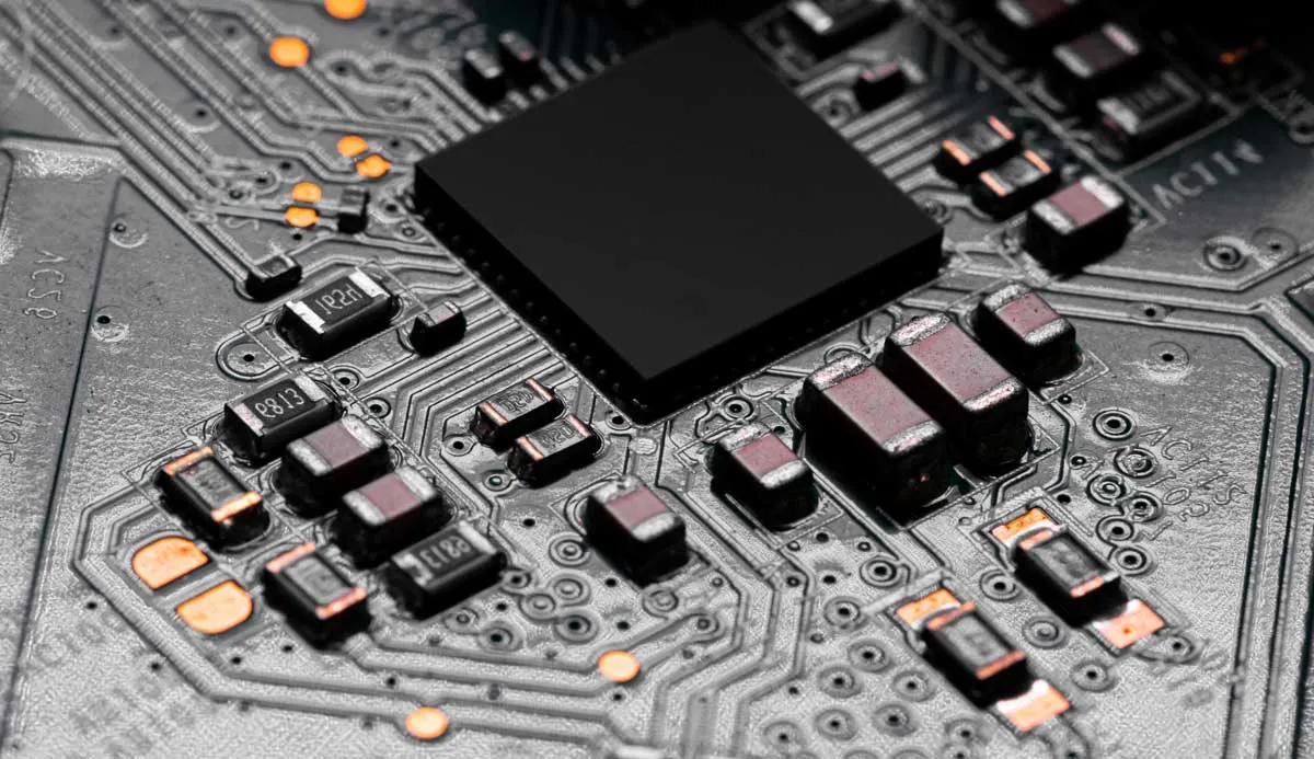
1. Size and Packaging
Components for compact gaming PCBs must have small footprints. Surface-mount technology (SMT) is the standard, with packages like 0201 (0.6mm x 0.3mm) for resistors and capacitors being common in portable devices. For integrated circuits, ball grid array (BGA) packages with fine pitch (as low as 0.4mm) allow for high pin counts in a small area, ideal for processors and memory chips used in gaming hardware.
2. Power Efficiency
Portable gaming devices rely on batteries, so power efficiency is critical. Selecting low-power components, such as voltage regulators with high efficiency (above 90%), can extend battery life without sacrificing performance. For example, using a step-down converter with a quiescent current below 50μA ensures minimal power draw during idle states.
3. Compatibility with High-Density Layouts
Components must be compatible with the tight spacing and multilayer routing of HDI PCBs. This means choosing parts with minimal parasitic effects and ensuring they can withstand the reflow soldering temperatures used in compact board assembly. Datasheets and manufacturer guidelines are invaluable during this selection process to avoid mismatches.
Best Practices for Designing Miniaturized PCBs for Gaming
To wrap up, here are some best practices for creating miniaturized PCBs tailored for portable gaming devices. These tips combine the techniques and considerations discussed above into actionable steps.
- Start with a Detailed Plan: Use design software to simulate layouts and identify potential issues like signal interference or thermal hotspots before prototyping.
- Prioritize Layer Stacking: Optimize the number of layers in HDI designs to balance cost and performance, typically using 4 to 8 layers for gaming PCBs.
- Test Iteratively: Build and test multiple prototypes to refine the design, focusing on signal integrity and thermal performance in real-world gaming scenarios.
- Collaborate with Manufacturers: Work closely with fabrication partners to ensure the design aligns with manufacturing capabilities, especially for microvias and fine traces.
- Stay Updated on Technology: Keep an eye on advancements in materials and manufacturing processes that can further enhance miniaturization efforts.
Conclusion: The Future of Miniaturization in Gaming PCBs
Miniaturization techniques for portable gaming device PCBs are transforming the way we experience gaming on the go. By leveraging high-density PCB layouts for gaming, addressing compact PCB design challenges, making smart choices in component selection for small PCBs, and utilizing microvia technology in gaming applications, designers can create powerful yet compact systems. HDI PCB design considerations for gaming further ensure that performance and reliability are never compromised, even in the smallest footprints.
As technology continues to advance, the push for smaller, more efficient PCBs will only grow stronger. Staying ahead of the curve means adopting these miniaturization strategies and continuously refining designs to meet the demands of next-generation gaming devices. With the right approach, the possibilities for innovation in portable gaming are endless.