 ALLPCB


In the world of electronics, maintaining PCB signal integrity is crucial for ensuring reliable performance, especially in high-speed PCB design. One often overlooked factor that plays a major role in this is the PCB form factor. But how exactly does the shape and size of a PCB affect signal integrity? Simply put, the form factor influences trace lengths, component placement, and impedance characteristics, which can lead to issues like signal reflection and crosstalk if not managed properly. In this blog, we’ll dive deep into the relationship between PCB form factor signal integrity and explore practical ways to mitigate PCB signal integrity issues for optimal design outcomes.
What Is PCB Form Factor and Why Does It Matter?
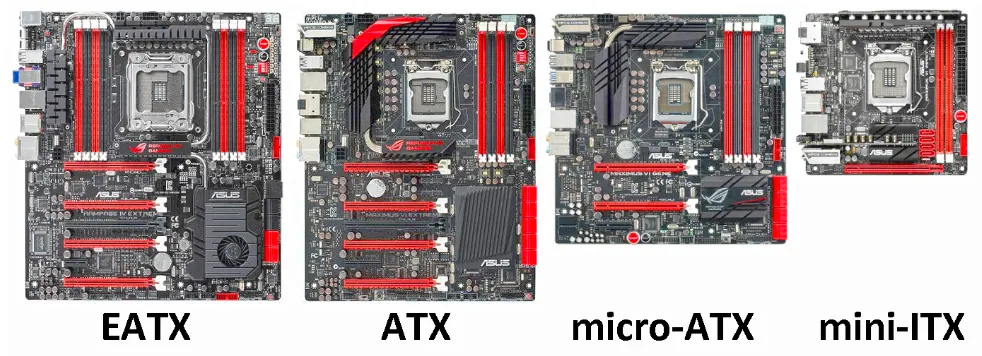
The term "PCB form factor" refers to the physical shape, size, and layout constraints of a printed circuit board. It dictates how much space is available for components, traces, and other design elements. Common form factors include ATX for motherboards, Micro-ATX for smaller systems, and custom shapes for specific applications like wearable devices or IoT gadgets.
Why does this matter for signal integrity? In high-speed PCB design, signals travel at speeds where even small changes in trace length or board dimensions can cause delays, reflections, or interference. A poorly chosen form factor can force designers to compromise on trace routing or component placement, leading to PCB signal integrity issues such as noise, crosstalk, or data loss. For instance, a compact form factor might require tightly packed traces, increasing the risk of electromagnetic interference (EMI).
Understanding Signal Integrity in High-Speed PCB Design
Before diving deeper into form factor impacts, let’s clarify what signal integrity means. Signal integrity refers to the quality of an electrical signal as it travels through a PCB. In high-speed PCB design, where signals operate at frequencies above 100 MHz or even into the GHz range, maintaining this quality becomes challenging. Issues like signal reflection, crosstalk, and impedance mismatches can distort signals, leading to errors or system failures.
Signal integrity is influenced by several factors, including trace length, dielectric materials, and board layout. The form factor ties into all of these by determining how much physical space you have to work with. A smaller form factor might limit your ability to maintain consistent impedance matching, while a larger one could introduce longer traces that increase signal delay.
How PCB Form Factor Impacts Signal Integrity
Let’s break down the specific ways in which PCB form factor affects signal integrity. Understanding these impacts can help designers make informed decisions during the planning stage.
1. Trace Length and Signal Delay
In high-speed PCB design, the length of traces directly affects signal timing. Longer traces result in greater signal delay, which can be problematic for synchronized signals like those in DDR memory or high-speed serial interfaces (e.g., PCIe, USB 3.0). A larger form factor often means longer traces to connect components across the board, increasing the risk of timing mismatches.
For example, if a signal travels along a trace at a speed of approximately 150 ps per inch (a common value for FR-4 material), a 10-inch trace introduces a delay of 1.5 ns. On a compact form factor, you might reduce this to a 2-inch trace with a delay of just 0.3 ns. Choosing the right form factor can minimize these delays and improve overall performance.
2. Component Placement and Crosstalk
The form factor also dictates where components can be placed on the board. In a smaller form factor, components are often packed closely together, increasing the risk of crosstalk—unwanted coupling of signals between adjacent traces. Crosstalk can degrade signal quality, especially at high frequencies where even a small amount of interference can cause errors.
To mitigate this, designers must carefully plan the layout, ensuring adequate spacing between high-speed traces. However, a constrained form factor might limit your options, making it harder to avoid PCB signal integrity issues like crosstalk.
3. Impedance Matching Challenges
Impedance matching is critical for preventing signal reflection in high-speed designs. Reflections occur when there’s a mismatch in impedance along a signal path, causing part of the signal to bounce back and interfere with the original transmission. The form factor influences impedance by affecting trace width, spacing, and the dielectric properties of the board stack-up.
For instance, a standard 50-ohm impedance for high-speed signals requires specific trace widths and layer thicknesses. On a smaller form factor, you might not have the space to maintain consistent trace widths or proper ground planes, leading to impedance variations. According to typical design rules, a trace width of 5 mils on a 1.6 mm FR-4 board with a ground plane can achieve 50 ohms, but deviations due to space constraints can push this value to 60 ohms or higher, causing reflections.
4. Power Distribution and Ground Planes
A solid ground plane is essential for maintaining signal integrity by providing a low-impedance return path for signals. However, the form factor can limit the size or continuity of ground planes, especially in compact or irregularly shaped boards. Discontinuities in the ground plane can lead to increased EMI and signal noise, undermining performance in high-speed PCB design.
For example, in a small form factor for a wearable device, you might need to split the ground plane to fit components, creating gaps that disrupt signal return paths. This can result in higher loop inductance and voltage drops, further contributing to PCB signal integrity issues.
Strategies to Optimize PCB Form Factor for Signal Integrity
Now that we’ve covered how form factor impacts signal integrity, let’s explore actionable strategies to address these challenges. These tips can help you design boards that balance physical constraints with performance requirements.
1. Choose the Right Form Factor Early
During the initial design phase, consider the signal speed and application requirements. If you’re working on a high-speed system like a 5G module or a data center server, opt for a form factor that allows enough space for proper trace routing and ground planes. For compact designs, prioritize modular form factors that let you separate high-speed sections onto smaller, dedicated boards.
2. Prioritize Short and Consistent Trace Lengths
Minimize trace lengths wherever possible to reduce signal delay and the risk of reflections. Use layout tools to match trace lengths for differential pairs or critical signals. For instance, in a design with a 2.5 GHz signal, a length mismatch of just 0.5 inches can cause a phase shift of over 10 degrees, leading to data errors. A form factor that supports direct, short connections between components can make this easier.
3. Implement Proper Impedance Control
Work with your PCB manufacturer to ensure consistent impedance matching across the board. Use simulation tools to calculate the required trace widths and layer stack-ups for your target impedance (e.g., 50 ohms for most high-speed signals). If the form factor limits your options, consider using thinner dielectric materials or microstrip traces to maintain control over impedance values.
4. Maximize Ground Plane Coverage
Even in small form factors, aim to maintain a continuous ground plane wherever possible. If splits are unavoidable, use stitching vias to connect ground layers and minimize disruptions in the return path. This helps reduce EMI and ensures stable signal performance in high-speed PCB design.
5. Simulate and Test Designs
Before finalizing your design, use signal integrity simulation tools to model how the form factor affects performance. Tools can predict issues like signal reflection or crosstalk based on trace geometry and board dimensions. After fabrication, test the board with high-speed signals to verify that it meets your requirements. For example, a time-domain reflectometer (TDR) can measure impedance discontinuities with an accuracy of ±1 ohm, helping you identify problem areas.
Real-World Examples of Form Factor Challenges
To illustrate these concepts, let’s look at two scenarios where form factor played a critical role in PCB signal integrity issues.
Scenario 1: Compact IoT Device
A team designing a wearable IoT device faced severe crosstalk due to the tiny form factor. With components packed into a 1-inch by 1-inch board, high-speed traces for a 2.4 GHz wireless module were placed too close together, resulting in signal interference. By revising the layout to use a slightly larger form factor and adding shielding vias, they reduced crosstalk by over 30%, ensuring reliable data transmission.
Scenario 2: Large Server Motherboard
In a server motherboard design, long traces across a large form factor caused significant signal delays for a 3.2 GHz memory bus. The team mitigated this by optimizing component placement to shorten critical paths and using length-matching techniques, cutting delay variations from 500 ps to under 100 ps.

Conclusion: Balancing Form Factor and Signal Integrity
The relationship between PCB form factor signal integrity is undeniable. Whether you’re dealing with a compact design for a portable gadget or a sprawling layout for a high-performance system, the form factor shapes your ability to maintain clean, reliable signals. By understanding the challenges—such as trace length delays, crosstalk, and impedance matching—and applying the strategies outlined above, you can crack the code of designing PCBs that perform flawlessly in high-speed PCB design.
At the heart of every successful design is careful planning. Take the time to evaluate your form factor choices early, simulate potential issues, and optimize your layout for signal integrity. With these steps, you’ll be well-equipped to tackle PCB signal integrity issues and deliver boards that meet the demands of today’s high-speed applications.


