 ALLPCB


In the fast-evolving world of wearable technology, choosing the right PCB form factor is crucial for designing devices that are compact, durable, and efficient. Whether you're working on a fitness tracker, smartwatch, or medical wearable, understanding wearable PCB design, flexible PCBs, rigid-flex PCBs, and small form factor PCBs can make or break your project. This guide will walk you through the essentials of PCB form factors for wearable tech electronics, helping you make informed decisions for your next innovation.
At its core, a PCB (Printed Circuit Board) form factor determines the shape, size, and flexibility of the board that powers your wearable device. For wearables, the challenge lies in balancing functionality with comfort and durability. In this comprehensive blog, we'll dive deep into the types of PCB form factors, their applications, design considerations, and best practices tailored for wearable technology. Let’s get started!
Why PCB Form Factors Matter in Wearable Technology
Wearable technology has unique demands compared to traditional electronics. Devices like smartwatches or health monitors must fit snugly on the body, endure constant movement, and operate efficiently in a tiny space. This is where PCB form factors come into play. The right form factor ensures that your device is lightweight, energy-efficient, and resilient to wear and tear.
For instance, a poorly designed PCB can lead to overheating, signal interference, or even physical breakage when bent or twisted during use. By focusing on small form factor PCBs and flexible designs, engineers can create wearables that are both powerful and user-friendly. In the sections below, we'll explore the key types of PCB form factors used in wearable tech and how they address these challenges.
Types of PCB Form Factors for Wearable Technology
When designing for wearable tech, you’ll typically encounter three main PCB form factors: rigid, flexible, and rigid-flex. Each has its strengths and ideal use cases. Let’s break them down.
1. Rigid PCBs: The Traditional Choice
Rigid PCBs are the standard in many electronics, made from solid, non-bendable materials like FR4 (a fiberglass-epoxy laminate). While they’re not the first choice for wearables due to their lack of flexibility, they can still be used in devices where durability and cost are priorities, and the form factor doesn’t require bending.
Pros:
- Cost-effective for mass production.
- High structural stability for mounting heavy components.
- Suitable for small, flat areas in wearables (e.g., a control module in a smartwatch).
Cons:
- Not ideal for curved or dynamic shapes.
- Can add unnecessary bulk to wearable designs.
For wearable tech, rigid PCBs are often used in small form factor PCB designs where space is limited but flexibility isn’t required. They’re best for static components that don’t need to conform to the body’s shape.
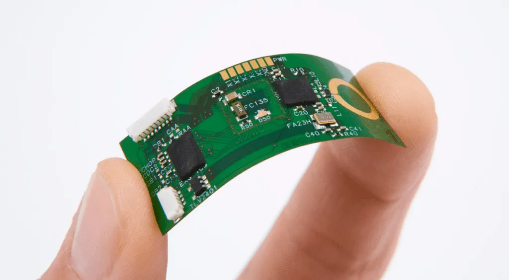
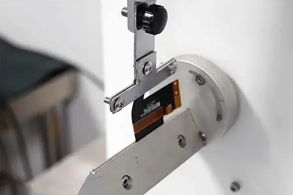
2. Flexible PCBs: Conforming to Curves
Flexible PCBs are a game-changer for wearable technology. Made from materials like polyimide, these boards can bend and flex without breaking, making them perfect for devices that wrap around the wrist or integrate into clothing.
Key Benefits:
- Lightweight and thin, ideal for compact wearables.
- Can conform to irregular shapes, improving comfort.
- Reduces the need for connectors, saving space and weight.
Applications: Flexible PCBs are widely used in fitness trackers and medical wearables, where the board must curve around the body. For example, a heart rate monitor might use a flexible PCB to fit seamlessly into a chest strap.
Design Tip: When working with flexible PCBs, ensure the bend radius is within the material’s limits (typically a minimum of 10 times the board thickness). Exceeding this can cause cracks or signal loss. For instance, a 0.1mm thick flexible PCB should have a bend radius of at least 1mm.
3. Rigid-Flex PCBs: The Best of Both Worlds
Rigid-flex PCBs combine rigid and flexible sections into a single board. This hybrid design offers the stability of rigid boards for mounting components and the adaptability of flexible boards for fitting into tight or curved spaces.
Advantages:
- Reduces assembly costs by eliminating connectors between rigid and flexible parts.
- Enhances reliability by minimizing points of failure.
- Perfect for complex wearables with both static and dynamic components.
Use Case: A smartwatch might use a rigid-flex PCB where the rigid section houses the processor and sensors, while the flexible section wraps around the wrist for a snug fit. According to industry data, rigid-flex designs can reduce device weight by up to 20% compared to using separate rigid and flexible boards.
Challenges: Rigid-flex PCBs are more expensive to manufacture due to their complex design and fabrication process. However, the trade-off is often worth it for high-performance wearables.
Key Considerations for Wearable PCB Design
Designing a PCB for wearable technology goes beyond just picking a form factor. Here are the critical factors to keep in mind during the wearable PCB design process to ensure functionality and user satisfaction.
1. Size and Miniaturization
Wearables demand small form factor PCBs to fit into tight spaces without compromising performance. Miniaturization is key, often requiring high-density interconnect (HDI) technology to pack more components into a smaller area.
Practical Tip: Use microvias (tiny holes with diameters as small as 0.1mm) to connect layers in HDI designs. This allows for tighter routing and smaller board sizes. For example, a smart ring might use an HDI PCB with a footprint of just 10mm x 10mm to house its sensors and battery management system.
2. Power Efficiency
Wearable devices often run on small batteries, so power efficiency is non-negotiable. Poor PCB design can lead to excessive power consumption, shortening battery life.
Design Strategy: Optimize trace widths and lengths to minimize resistance and power loss. For instance, a trace width of 0.2mm for a 1A current can keep voltage drops below 0.1V, preserving battery life. Additionally, place power-hungry components like processors closer to the power source to reduce impedance.
3. Durability and Flexibility
Wearables face constant movement and stress, so durability is critical, especially for flexible PCBs and rigid-flex PCBs. Repeated bending can cause fatigue in materials, leading to cracks or broken traces.
Best Practice: Use materials with high fatigue resistance, such as polyimide for flexible sections, and reinforce critical areas with stiffeners. Testing shows that polyimide-based flexible PCBs can withstand over 100,000 bend cycles at a 2mm radius without failure.
4. Signal Integrity
In wearable tech electronics, maintaining signal integrity is vital, especially with high-speed data from sensors or wireless communication modules. Small form factors and flexible designs can introduce noise or interference if not handled properly.
Solution: Keep high-speed signal traces short and straight, avoiding sharp bends in flexible areas. Use ground planes to shield against electromagnetic interference (EMI). For example, a Bluetooth module in a smartwatch might require a controlled impedance of 50 ohms for its traces to ensure reliable data transmission at speeds up to 2 Mbps.
Applications of PCB Form Factors in Wearable Technology
Different wearable devices have unique needs, and the choice of PCB form factor can significantly impact their performance. Here are some common applications and the best PCB types for each.
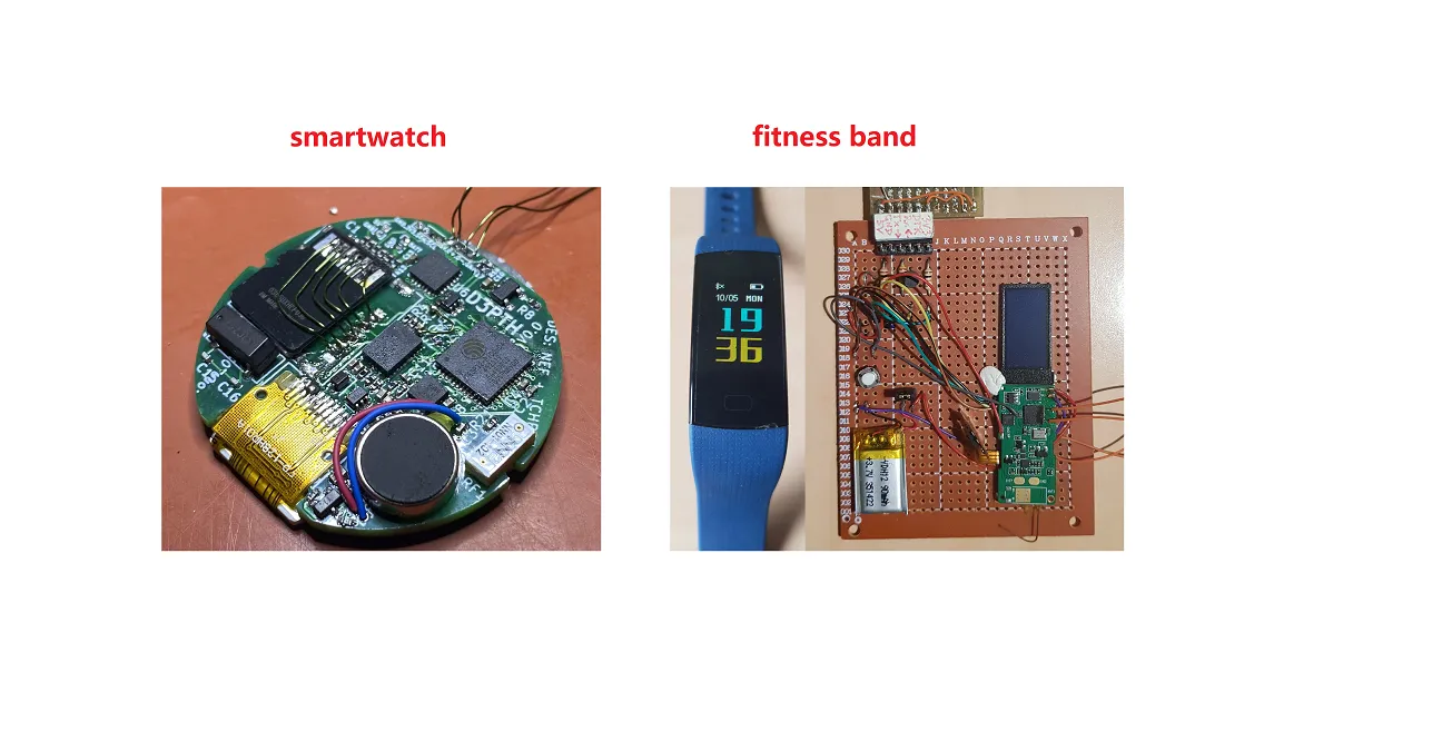
1. Fitness Trackers and Smartwatches
These devices need to be lightweight and comfortable, often requiring flexible PCBs or rigid-flex PCBs to wrap around the wrist. A typical smartwatch PCB might measure just 20mm x 30mm, with flexible sections for the band connection.
2. Medical Wearables
Medical devices like glucose monitors or ECG patches must adhere closely to the skin, making flexible PCBs ideal. These boards can be as thin as 0.05mm, ensuring minimal discomfort while maintaining accuracy in sensor readings.
3. Smart Clothing and Textiles
Emerging wearable tech like smart fabrics integrates electronics directly into clothing. Here, ultra-thin flexible PCBs are embedded into materials, allowing for washable and durable designs. Conductive traces in these PCBs often use silver ink with a resistance as low as 0.01 ohms per square for reliable performance.
Best Practices for Designing PCBs for Wearable Tech
To wrap up, here are actionable tips to optimize your wearable PCB design process:
- Prioritize Space Efficiency: Use multilayer designs in small form factor PCBs to stack components vertically, saving horizontal space.
- Test for Flexibility: Simulate real-world bending and twisting during the design phase to ensure flexible PCBs won’t fail under stress.
- Optimize for Manufacturing: Work closely with your PCB fabrication team to balance cost and performance, especially for complex rigid-flex PCBs.
- Focus on Thermal Management: Wearables are close to the skin, so use low-power components and heat-dissipating layouts to avoid overheating. For example, keep heat-generating ICs away from skin-contact areas.
Conclusion: Crafting the Future of Wearable Technology
The right PCB form factor is the backbone of any successful wearable device. Whether you’re leveraging the adaptability of flexible PCBs, the hybrid power of rigid-flex PCBs, or the compactness of small form factor PCBs, understanding these options empowers you to design cutting-edge wearable tech electronics. By focusing on size, durability, power efficiency, and signal integrity in your wearable PCB design, you can create products that are not only functional but also comfortable and reliable for users.
As wearable technology continues to grow, staying ahead means mastering the art and science of PCB design. With the insights and tips shared in this guide, you’re well-equipped to tackle the challenges and innovate in this exciting field. Let’s build the future of wearables, one circuit at a time!


