ALLPCB


In the realm of PCB design, especially for power applications, understanding the creepage impact of lead forming for through-hole components is crucial. Creepage, the shortest path along the surface of an insulating material between two conductive parts, plays a vital role in ensuring safety and reliability in power designs. Improper lead forming can reduce creepage distances, increasing the risk of electrical breakdown or arcing, particularly in high-voltage environments. In this comprehensive guide, we’ll explore how lead forming affects creepage, why it matters for through-hole components in power designs, and best practices to mitigate risks.
What is Creepage and Why Does It Matter in Power Designs?
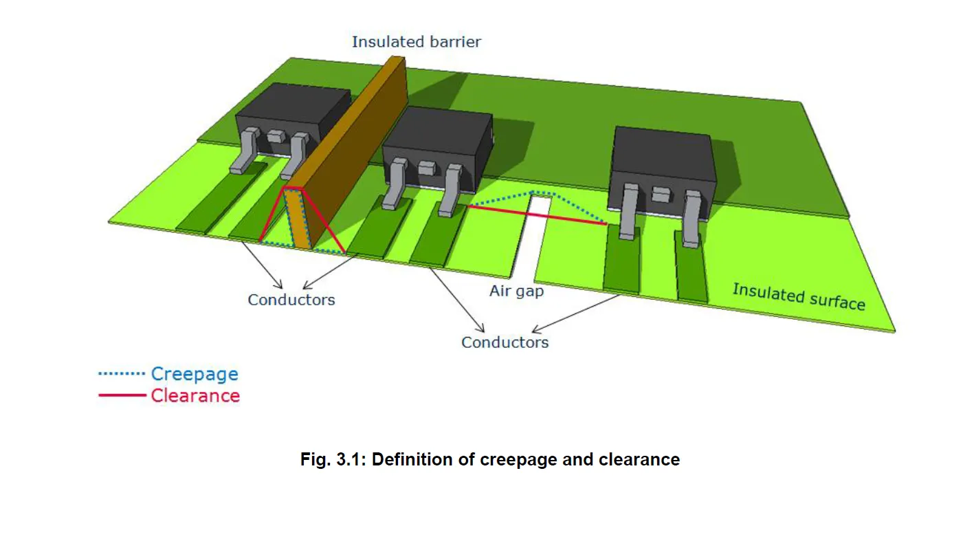
Creepage refers to the distance along the surface of a PCB or insulating material between two conductive elements, such as component leads or traces. Unlike clearance, which measures the shortest distance through air, creepage focuses on surface paths where contaminants like dust, moisture, or pollution can lower insulation resistance and lead to electrical failure.
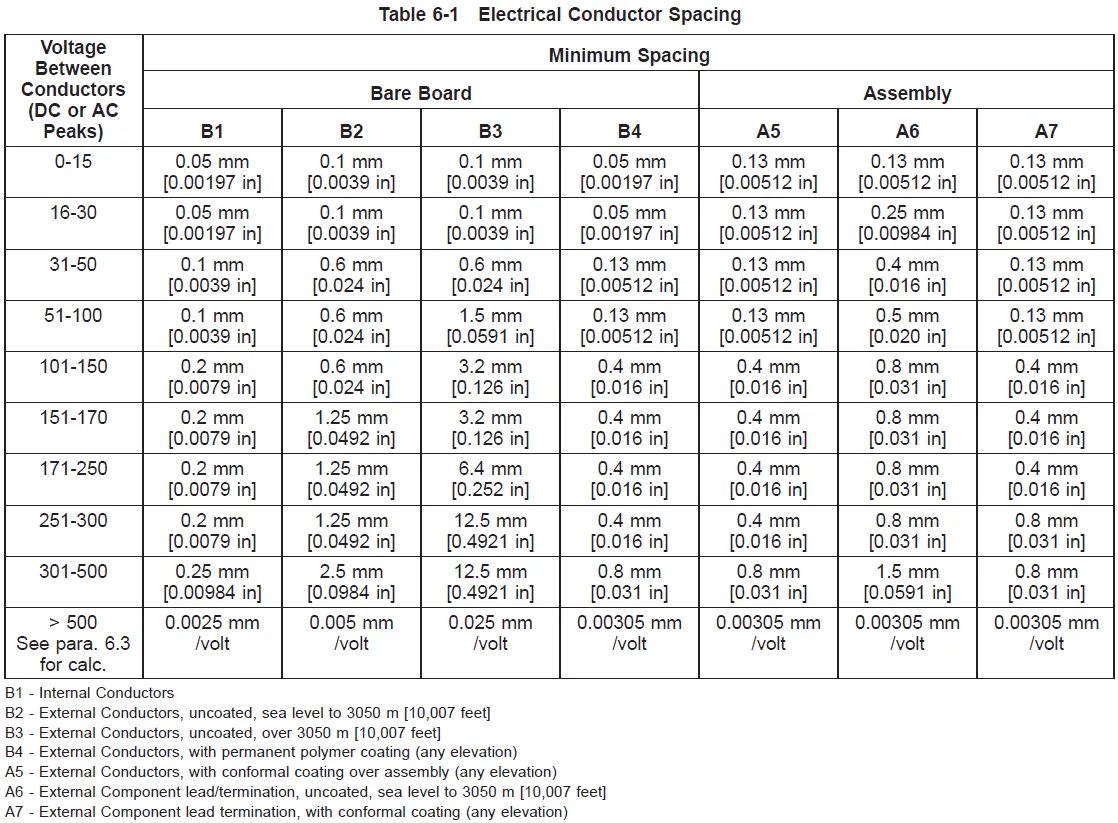
In power designs, where voltages can range from hundreds to thousands of volts, maintaining adequate creepage distances is essential to prevent arcing, short circuits, and safety hazards. For instance, in a 500V power supply design, a creepage distance of at least 6mm might be required depending on the pollution degree and material properties, as per standards like IEC 60950 or IPC-2221. Failing to account for creepage can result in catastrophic failures, especially in environments with high humidity or contamination.
The Role of Through-Hole Components in Power Designs
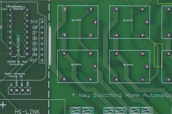
Through-hole components are widely used in power electronics due to their robustness and ability to handle high currents and voltages. Components like transformers, large capacitors, and power resistors often rely on through-hole mounting for secure mechanical connections and effective heat dissipation. For example, a through-hole electrolytic capacitor in a 48V DC-DC converter can handle currents exceeding 10A, making it ideal for such applications.
However, the leads of these components, which pass through the PCB and are soldered on the opposite side, can introduce challenges related to creepage. The proximity of leads to other conductive elements, such as adjacent pads or traces, must be carefully managed to avoid compromising safety distances.
How Lead Forming Affects Creepage in PCB Designs
Lead forming is the process of bending or shaping the leads of through-hole components to fit the PCB layout or to meet specific mechanical or thermal requirements. While this process is often necessary for proper component placement and stress relief, it can significantly impact creepage distances in the following ways:
- Reduced Surface Distance: Bending leads too close to other conductive elements can shorten the creepage path. For instance, if a lead is bent at a sharp angle near a neighboring pad, the effective surface distance might drop below the required 4mm for a 300V application, increasing the risk of arcing.
- Stress on Insulation: Improper lead forming can create mechanical stress points on the PCB or component, potentially cracking the insulating material and further reducing creepage effectiveness.
- Contaminant Accumulation: Bent leads can create small crevices or gaps where dust and moisture accumulate, lowering the insulation resistance over time and making creepage violations more likely.
Key Factors Influencing Creepage in Lead Forming
Several factors determine how lead forming impacts creepage in PCB through-hole designs for power applications. Understanding these factors can help engineers design safer and more reliable boards:
1. Voltage Levels
Higher voltages demand greater creepage distances. For example, a design operating at 1000V may require a creepage distance of 8mm or more, depending on the environment. Lead forming must ensure that bent leads do not encroach on this critical spacing.
2. Pollution Degree
The pollution degree, as defined by standards like IEC, indicates the level of contamination expected in the operating environment. A pollution degree of 3 (conductive pollution or high humidity) requires larger creepage distances compared to a cleaner environment (pollution degree 1). Lead forming must account for these conditions to prevent surface tracking.
3. Material Properties
The Comparative Tracking Index (CTI) of the PCB material affects how well it resists surface tracking. Materials with a higher CTI (e.g., FR-4 with CTI of 175) can support smaller creepage distances, but lead forming must still avoid creating stress points that degrade the material over time.
4. Altitude
At higher altitudes, air pressure decreases, reducing the dielectric strength of air and potentially affecting clearance. While creepage is less directly impacted, designs for high-altitude applications must consider combined effects on lead positioning and spacing.
Best Practices for Lead Forming to Minimize Creepage Issues
To ensure that lead forming does not compromise creepage in power designs, follow these actionable best practices:
1. Maintain Minimum Creepage Distances
Always refer to industry standards like IPC-2221 or IEC 60950 to determine the minimum creepage distance for your design’s voltage and environmental conditions. For a 600V system in a pollution degree 2 environment, a creepage distance of at least 6.4mm is often recommended. Use PCB design software to check distances after lead forming.
2. Use Proper Lead Bending Techniques
Avoid sharp bends or excessive force when forming leads, as this can damage the component or PCB. Use tools like lead-forming jigs to achieve consistent bends, ensuring that leads are at least 2-3mm away from adjacent conductive elements to maintain creepage.
3. Incorporate Slots or Barriers
For high-voltage designs, consider adding slots or physical barriers in the PCB between leads to increase the effective creepage path. A slot width of 1mm can significantly enhance safety by preventing surface tracking, even if leads are closer together.
4. Optimize Component Placement
During the layout phase, position through-hole components to maximize natural creepage distances before lead forming. For example, place high-voltage components like MOSFETs or capacitors on opposite sides of the board if possible, reducing the need for tight lead bends.
5. Test and Validate Designs
After lead forming and assembly, perform high-potential (Hi-Pot) testing to verify that creepage distances are sufficient under operating conditions. A typical Hi-Pot test for a 500V design might apply 2500V for one minute to check for breakdown across creepage paths.
Common Mistakes in Lead Forming and Creepage Management
Even experienced engineers can make errors when handling PCB through-hole components in power designs. Here are some pitfalls to avoid:
- Overlooking Environmental Factors: Failing to account for humidity or pollution can lead to insufficient creepage distances. A design that works in a lab may fail in a humid industrial setting if creepage is not adjusted accordingly.
- Ignoring Lead Stress: Excessive bending can weaken leads, causing them to break or shift over time, potentially reducing creepage distances during operation.
- Inadequate Spacing in High-Density Designs: In compact power designs, the temptation to minimize spacing can lead to creepage violations. Always prioritize safety over board size when dealing with high voltages.
The Importance of Standards and Compliance in Creepage Design
Adhering to international standards is non-negotiable for power designs. Standards like IPC-2221 provide detailed guidelines on creepage and clearance based on voltage, material, and environment. For instance, a 300V design on FR-4 material in a pollution degree 2 environment typically requires a creepage distance of 3.2mm. Compliance ensures not only safety but also reliability and market acceptance of your product.
Additionally, standards help in designing for worst-case scenarios. If your power design operates at 400V but could experience transient spikes to 600V, base your creepage calculations on the higher value to account for overvoltage conditions.
Conclusion: Balancing Lead Forming and Creepage for Reliable Power Designs
The creepage impact of lead forming for through-hole components in power designs is a critical consideration that can make or break the safety and performance of a PCB. By understanding how lead forming affects surface distances, adhering to industry standards, and implementing best practices, engineers can design boards that withstand high voltages and harsh environments without compromising reliability.
Whether you’re working on a 48V DC-DC converter or a 1000V industrial power supply, always prioritize creepage distances during the lead forming process. Use proper tools, validate your designs through testing, and leverage PCB layout techniques like slots or barriers to enhance safety. With careful attention to detail, you can ensure that your power designs remain robust and compliant for years to come.