 ALLPCB


If you're diving into the world of blockchain technology and want to design hardware to support it, you’ve come to the right place. This guide will walk you through the basics of creating a printed circuit board (PCB) for blockchain hardware, focusing on secure and efficient circuit design. Whether you're a hobbyist or a beginner engineer, you'll learn the essentials of PCB design, key components, and tips to ensure your blockchain project is both functional and safe.
In this detailed blog, we’ll break down everything you need to know about basic PCB design, provide a blockchain hardware tutorial, explore secure circuit design, offer an electronic components guide, and inspire ideas for a hobbyist blockchain project. Let’s get started on building circuits that power the future of decentralized technology!
What Is Blockchain Hardware and Why Does PCB Design Matter?
Blockchain technology is a decentralized system for securely recording transactions across a network. While most people associate blockchain with software like cryptocurrencies, hardware plays a critical role in ensuring the system’s efficiency and security. Blockchain hardware includes devices like mining rigs, secure wallets, and nodes that validate transactions.
A well-designed PCB is the backbone of such hardware. It connects electronic components, ensures reliable performance, and protects sensitive data from tampering or interference. Poor PCB design can lead to signal loss, overheating, or even security vulnerabilities—issues you can’t afford in blockchain applications where trust and uptime are paramount.
In this guide, we’ll cover how to design a PCB that meets the unique demands of blockchain hardware, balancing efficiency with robust security measures.
Understanding Basic PCB Design for Blockchain Hardware
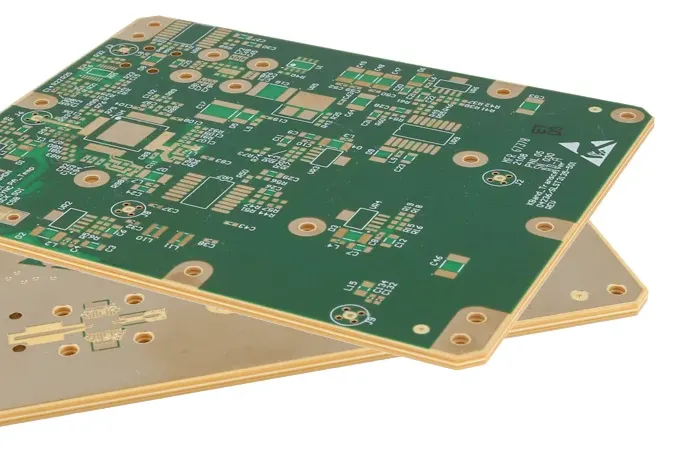
Before diving into the specifics of blockchain hardware, let’s cover the fundamentals of PCB design. A PCB, or printed circuit board, is a flat board that holds and connects electronic components using conductive copper tracks. It’s the foundation of almost every electronic device, including those used in blockchain systems.
For beginners, the key elements of basic PCB design include:
- Layers: Most PCBs have multiple layers of copper tracks separated by insulating material. Simple projects may use a single or double-layer board, while complex blockchain hardware might need 4-6 layers to handle high-speed signals.
- Traces: These are the copper pathways that carry electrical signals between components. Trace width and spacing are critical to avoid interference, especially in high-frequency blockchain mining circuits where signals can reach speeds of 100 MHz or more.
- Vias: Small holes that connect traces between layers. Proper placement of vias ensures smooth signal flow and reduces noise.
- Ground Planes: A large copper area connected to ground helps reduce electrical noise and provides a stable reference for signals—an essential feature for secure circuit design in blockchain hardware.
Designing a PCB for blockchain hardware requires extra attention to power management and heat dissipation since devices like mining rigs often run 24/7 under heavy loads. For example, a typical mining ASIC (Application-Specific Integrated Circuit) can draw up to 150W of power, generating significant heat that must be managed through proper PCB layout and thermal vias.

Step-by-Step Blockchain Hardware Tutorial: Designing Your First PCB
Now that you understand the basics, let’s walk through the steps to design a PCB for blockchain hardware. This tutorial is tailored for beginners and hobbyists looking to build a simple blockchain node or hardware wallet.
Step 1: Define Your Hardware Requirements
Start by deciding what your blockchain hardware will do. For a hobbyist blockchain project, you might design a small node that connects to a network and validates transactions. Key requirements could include a microcontroller (MCU) for processing, a secure storage chip for private keys, and a communication module like Wi-Fi or Ethernet.
Step 2: Choose the Right Components
Select components that balance performance, cost, and security. For example:
- Microcontroller: An ARM-based MCU with at least 100 MHz clock speed can handle basic blockchain operations.
- Secure Element: Use a chip like a Trusted Platform Module (TPM) to store cryptographic keys securely.
- Power Management: Include a voltage regulator to supply a stable 3.3V or 5V to sensitive components.
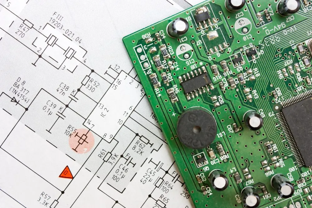
Step 3: Create a Schematic
Draw a schematic diagram that shows how components connect. Use design software to map out power lines, ground connections, and signal paths. Ensure that high-speed signals (like those from a communication module) have short, direct traces to minimize interference.
Step 4: Design the PCB Layout
Translate your schematic into a physical layout. Place components logically—keep power-hungry parts like processors near voltage regulators, and separate analog and digital sections to avoid noise. Maintain trace impedance around 50 ohms for high-speed signals to prevent signal degradation.
Step 5: Test and Iterate
After manufacturing your PCB, test it for functionality. Use a multimeter to check for short circuits and verify that signals are clean using an oscilloscope if possible. If issues arise, revise your design and produce a new prototype.
Secure Circuit Design: Protecting Your Blockchain Hardware
Security is non-negotiable in blockchain hardware. A single vulnerability can compromise private keys or transaction data, leading to significant losses. Here are key principles for secure circuit design:
Isolate Sensitive Components
Physically separate secure elements (like cryptographic chips) from other parts of the circuit. Use dedicated ground planes and shielding to prevent electromagnetic interference (EMI) that could leak sensitive data. For instance, side-channel attacks can detect power fluctuations as low as 0.1mV to infer encryption keys if not properly shielded.
Implement Power Monitoring
Add circuits to detect abnormal power usage, which could indicate tampering. A simple comparator circuit can trigger a shutdown if voltage drops below 2.8V or spikes above 5.5V on a 3.3V system.
Minimize Attack Surfaces
Reduce the number of exposed pins or test points on your PCB. Unused pins on a microcontroller should be grounded or disabled in firmware to prevent attackers from probing them.
Electronic Components Guide for Blockchain PCBs
Choosing the right components is critical for a successful blockchain hardware project. Here’s a beginner-friendly guide to essential components:
- Microcontrollers (MCUs): Look for MCUs with built-in cryptographic accelerators. A clock speed of 80-120 MHz is sufficient for most small-scale projects.
- Secure Storage Chips: These protect private keys and sensitive data. Chips with hardware-based encryption are ideal for blockchain applications.
- Communication Modules: For nodes, use Ethernet or Wi-Fi modules with support for secure protocols like TLS. Ensure a data rate of at least 10 Mbps for smooth network communication.
- Capacitors and Resistors: Use decoupling capacitors (e.g., 0.1 μF) near power pins of ICs to filter noise. Resistors in the range of 1-10 kΩ are often used for pull-up or pull-down configurations.
- Thermal Management: Add heat sinks or thermal pads for high-power components. Ensure thermal vias are placed near hot spots to dissipate heat effectively.
When sourcing components, prioritize reliability over cost. A failed component in a blockchain device can lead to downtime or security breaches, costing far more than the price of a higher-quality part.
Inspiring a Hobbyist Blockchain Project: Build a Simple Node
For hobbyists, a great starting point is designing a simple blockchain node that connects to a test network. This project lets you apply basic PCB design principles while learning about blockchain technology.
Project Overview: Create a small device that runs blockchain node software, validates transactions, and communicates with other nodes. You’ll need a microcontroller, a secure storage chip, and a basic communication module.
Key Steps:
- Design a PCB to host your components, ensuring a stable power supply with a 3.3V regulator.
- Program the microcontroller to sync with a blockchain test network and store data securely.
- Add an LED indicator to show network status—green for connected, red for offline.
This project is not only educational but also scalable. Once you master the basics, you can upgrade to more powerful hardware or add features like a display for real-time transaction data.
Tips for Efficient and Reliable PCB Design
To wrap up, here are some practical tips to ensure your blockchain hardware PCB is both efficient and reliable:
- Optimize Power Distribution: Use wide traces for power lines (at least 20-30 mils) to handle high currents without voltage drops.
- Plan for Scalability: Leave extra space on your PCB for future upgrades or additional components.
- Use Simulation Tools: Before manufacturing, simulate your design to check for signal integrity issues or thermal problems.
- Focus on Documentation: Keep detailed notes on your schematic and layout. This makes troubleshooting or revising your design much easier.
Conclusion: Start Your Blockchain Hardware Journey Today
Designing a PCB for blockchain hardware might seem daunting, but with the right approach, it’s an achievable and rewarding task. By mastering basic PCB design, following a blockchain hardware tutorial, prioritizing secure circuit design, using this electronic components guide, and experimenting with a hobbyist blockchain project, you can create hardware that supports the future of decentralized technology.
At ALLPCB, we’re passionate about helping engineers and hobbyists bring their ideas to life. Whether you’re just starting out or refining an advanced design, our resources and expertise are here to support you every step of the way. Dive into your blockchain hardware project today and build circuits that are secure, efficient, and ready for the challenges of tomorrow.


