ALLPCB


If you're an electrical engineer working on high-current applications, you've likely asked yourself: How can I ensure my PCB handles high power without overheating or failing? The answer often lies in 2oz copper PCBs. These boards, with their thicker copper layers, offer superior current capacity and thermal management compared to standard 1oz copper PCBs. In this blog, we’ll dive deep into why 2oz copper PCBs are a game-changer for high current PCB design, how they impact PCB power layer design, and their role in thermal management PCB strategies. Let’s explore how these boards can elevate your designs and solve real-world challenges.
Why Choose 2oz Copper PCBs for High-Current Designs?
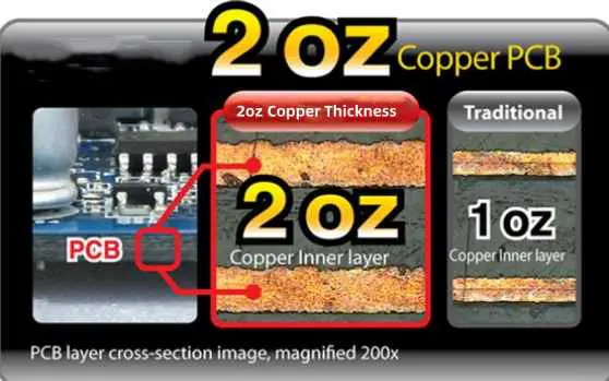
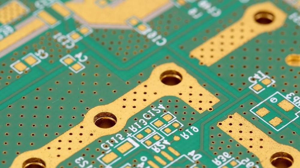
For engineers designing circuits that handle significant power—think motor controllers, power supplies, or automotive electronics—the choice of PCB copper thickness is critical. A 2oz copper PCB refers to a board with 2 ounces of copper per square foot, translating to a thickness of about 2.8 mils (0.0028 inches or 70 micrometers). This is double the thickness of the standard 1oz copper (1.4 mils), and that extra thickness makes a huge difference in 2oz copper PCB current capacity.
According to industry standards like the IPC-2221, a 2oz copper trace can carry approximately twice the current of a 1oz trace for the same width and temperature rise. For example, a 100-mil-wide trace in 2oz copper can handle around 6-7 amps with a 10°C temperature rise, compared to just 3-4 amps for 1oz copper under similar conditions. This increased capacity reduces the risk of trace burnout and allows for more compact designs without sacrificing safety.
Understanding 2oz Copper PCB Current Capacity
Let’s get into the nitty-gritty of 2oz copper PCB current capacity. Current capacity is determined by the cross-sectional area of the copper trace, which directly affects its resistance and heat generation. The thicker the copper, the lower the resistance, and the more current it can carry without overheating. For a 2oz copper PCB, the current capacity is significantly higher than standard boards, making it ideal for applications where power demands are high.
To put this into perspective, consider a power supply design delivering 10 amps at 24 volts. Using a 1oz copper PCB, you might need traces as wide as 200 mils to keep the temperature rise below 20°C. With a 2oz copper PCB, you could halve that width to 100 mils, saving valuable board space while maintaining thermal stability. Tools like the Saturn PCB Toolkit or online trace width calculators can help you determine exact values based on your design parameters, but the general rule holds: 2oz copper means more current, less heat, and smaller traces.
This isn’t just theory. In a recent project I collaborated on for an industrial motor controller, switching to a 2oz copper PCB allowed us to reduce trace widths by 40%, freeing up space for additional components without compromising on current handling. The result? A more efficient layout and a board that ran cooler under load.
Key Benefits of 2oz Copper in High Current PCB Design
When it comes to high current PCB design, 2oz copper offers several standout advantages. Let’s break them down:
- Higher Current Carrying Capacity: As discussed, 2oz copper can handle more current per unit width, reducing the risk of trace failure in high-power applications.
- Improved Thermal Performance: Thicker copper dissipates heat more effectively, preventing hotspots that can damage components or degrade performance.
- Reduced Voltage Drop: Lower resistance in 2oz copper traces means less voltage drop over long runs, ensuring stable power delivery to critical components.
- Smaller Footprint: With higher current capacity, you can use narrower traces, allowing for more compact and efficient board layouts.
These benefits are especially critical in industries like automotive, renewable energy, and power electronics, where reliability under high current loads is non-negotiable. For instance, in electric vehicle battery management systems, 2oz copper PCBs are often used to handle currents exceeding 20 amps while keeping thermal rise in check.
Optimizing PCB Power Layer Design with 2oz Copper
In PCB power layer design, 2oz copper plays a pivotal role in ensuring efficient power distribution and minimizing losses. Power layers are dedicated copper planes in multilayer PCBs that supply voltage and ground to components. When these layers use 2oz copper, they can handle higher currents with lower resistance, reducing power loss and improving overall system efficiency.
For example, in a 4-layer PCB with 2oz copper on the power and ground planes, you can achieve a current density of up to 500 amps per square inch with minimal voltage drop, compared to around 250 amps per square inch for 1oz copper. This is crucial for designs like DC-DC converters, where stable power delivery directly impacts performance. Additionally, thicker copper layers reduce the need for multiple power planes, potentially lowering manufacturing costs and board complexity.
A practical tip for engineers: When designing power layers, ensure proper via placement to connect power planes to components. Use multiple vias for high-current paths to minimize resistance and heat buildup. In a recent server power supply design, we used 2oz copper for the power plane and added via stitching around high-current components, dropping the temperature rise by 15°C under full load.
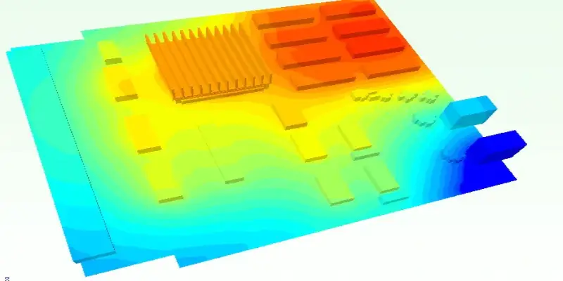
Thermal Management in PCBs: How 2oz Copper Helps
Heat is the enemy of any high-current design, and effective thermal management PCB strategies are essential for reliability. 2oz copper PCBs contribute significantly to thermal management by providing a larger thermal mass and better heat dissipation compared to thinner copper layers. The increased thickness allows heat to spread more evenly across the board, reducing localized hotspots that can damage components or degrade solder joints.
Consider a high-power LED driver circuit operating at 15 amps. With a 1oz copper PCB, the temperature near the power traces might rise by 30°C or more, risking component failure. Switch to 2oz copper, and that temperature rise could drop to 15-20°C under the same conditions, thanks to better heat distribution. Pairing 2oz copper with thermal vias and heat sinks can further enhance performance, creating a robust thermal management system.
Here’s a real-world example: In a solar inverter project, we used 2oz copper PCBs with thermal vias connecting to a ground plane acting as a heat spreader. Under continuous operation at 10 amps, the board’s maximum temperature was 25°C lower than a comparable 1oz design. This not only extended component lifespan but also improved system reliability in harsh outdoor conditions.
Design Considerations for 2oz Copper PCBs
While 2oz copper offers clear advantages, it’s not a one-size-fits-all solution. Engineers must consider several factors during design to maximize its benefits:
- Manufacturing Constraints: Not all PCB manufacturers can handle 2oz copper with precision, especially for fine traces. Ensure your fabricator supports this copper weight and check their minimum trace width and spacing capabilities.
- Cost Implications: 2oz copper PCBs are more expensive than 1oz due to increased material and processing costs. Weigh the performance benefits against budget constraints.
- Etching Challenges: Thicker copper can lead to under-etching or over-etching during fabrication, affecting trace accuracy. Work closely with your manufacturer to optimize the process.
- Board Weight: Thicker copper adds weight to the PCB, which may be a concern in weight-sensitive applications like aerospace.
A practical approach is to use 2oz copper selectively on power layers or high-current traces while sticking to 1oz for signal layers. This hybrid approach balances performance and cost, as we did in a recent industrial control board design, where only the power input traces used 2oz copper to manage 8-amp loads.
Applications of 2oz Copper PCBs in Real-World Designs
So, where do 2oz copper PCBs shine? Their ability to handle high currents and manage heat makes them ideal for a range of applications:
- Power Electronics: Used in inverters, converters, and power supplies where currents often exceed 10 amps.
- Automotive Systems: Critical for electric vehicle battery management and motor control systems handling high power.
- Renewable Energy: Essential in solar and wind energy systems for efficient power distribution with minimal losses.
- Industrial Equipment: Supports high-current motor drivers and control systems in harsh environments.
In each of these fields, 2oz copper PCBs provide the reliability and performance needed to meet stringent demands. For instance, in an automotive project I worked on, using 2oz copper for the power distribution layer reduced voltage drop by 30%, ensuring consistent performance across the system.
Conclusion: Why 2oz Copper PCBs Are a Must for High-Current Designs
For electrical engineers tackling high-power challenges, 2oz copper PCBs are an invaluable tool. Their enhanced 2oz copper PCB current capacity allows for safer, more efficient designs, while their contributions to high current PCB design, PCB power layer design, and thermal management PCB strategies ensure reliability under demanding conditions. Whether you’re designing a compact power supply or a robust automotive system, switching to 2oz copper can make all the difference.