 ALLPCB


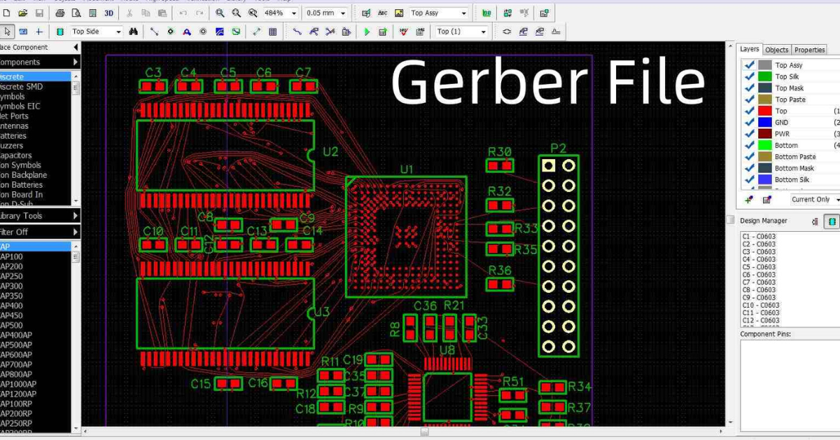
Circuit boards hold a crucial role in the field of electronics. To create these PCBs properly, we depend heavily on Gerber files. These serve as instructions to machines responsible for crafting every layer of PCB with precision and accuracy. If there are no Gerber files, making a PCB precisely according to the designer's intent cannot be achieved.
1. Gerber Files
2. Why are they important in PCB design?
3. And the way to make them using various PCB design programs.
It offers recommendations on examining and sending Gerber files too. In this article, the kinds of Gerber file formats will be discussed, along with their compatibility with ALLPCB software. By the end, you will understand how to produce, view, and verify Gerber files.
Further Reading: Gerber File Viewers: How to Ensure Error-Free PCB Fabrication
What Is a Gerber File?
A Gerber file is a computer file used for making PCB. It has information to guide the production of all layers in a PCB. These files are 2D coordinate data that give details about each layer of the PCB. They define traces, holes, pads, silkscreen, and other essential elements.
The format of the Gerber file was made in the 1960s. It was named by H. Joseph Gerber, the person who made it, after his name. Since then, Gerber files have become standard in the printed circuit board industry. Almost every PCB design software is compatible with Gerber files. This universal format enables manufacturers to create a PCB according to the intentions of the designer.
Why Are Gerber Files Important?
Gerber files are necessary for the accurate manufacture of PCBs. These files supply precise directions for every portion of the PCB. It is these documents that manufacturers use to instruct their machinery on what needs doing. Small mistakes in Gerber files can result in troubles with the final PCB. Such problems may imply shorts, disconnected links, or lost components.
When designers make proper Gerber files, they assist manufacturers in preventing errors. It also cuts down on production hold-ups and minimizes expenses. Without these Gerber files, every PCB would need specific instructions, which could hinder mass production.
Structure of a Gerber File
A Gerber file gets its structure from numerous layers. Every layer contains unique information. All these layers together supply all the necessary data for making a PCB.
Here are the primary components in a Gerber file:
1. Configuration Parameters
2. Aperture Definitions
3. XY Coordinates
4. Draw and Flash Commands
1. Configuration Parameters
Setting the basic attributes of the PCB requires configuration parameters. These parameters contain information such as resolution, scaling, and units.
The definition of resolution is how correctly the board production can be achieved. If resolution is high, it indicates more exactness. This becomes very vital for circuits that have extremely small details.
The units in the setup can be either millimeters or inches. To get precise measurements, it is important to use consistent units.
Scaling influences the dimension of elements on the board. It assures that every detail is made at the proper scale.
Setting parameters functions like the foundation of a blueprint. They direct the machine to understand the data in an appropriate manner. If configuration is not done correctly, it could lead to misinterpretation of output.
2. Aperture Definitions
The definition of the aperture determines the forms utilized in the PCB layout. These forms are known as apertures. Every single aperture represents a distinctive characteristic, such as a line or pad.
The shape of apertures, like circles, rectangles, or unique forms, can change based on the design of the PCB.
Also, the sizes of every hole are specified. For example, a pad could have a width of 0.5 mm and on the other hand, a line might be 0.2 mm in thickness.
Every hole is given a specific code, known as an aperture code. The device utilizes these codes to recognize and generate each characteristic.
Definitions of aperture help in creating complex designs with ease. They enable the machine to generate precise shapes. In the absence of these definitions, the machine would struggle to reproduce various features.
Recommended Reading: Design Rule Check (DRC): Avoiding Common PCB Layout Mistakes
3. Geometric Templates
Fundamental geometric templates are apertures that determine how circuit board features are created. They're like digital stencils that determine what goes on where on a printed circuit board. The most common aperture shape is circles, used to produce round pads and through holes.
This doesn't mean that designers are limited to circular shapes. Rectangular pads and specialized connectors are excellent candidates for use with rectangles. More complex geometric configurations are permitted by polygon apertures.
These apertures are defined in the Gerber file using certain D codes. A simple example would be defined as %ADD10C0.020*%. This is a circular aperture with a 0.020 inch diameter. These aperture definitions are very precise.
Finer circuit details are achieved with smaller apertures. This has a direct influence on the circuit board design complexity and density.
4. XY Coordinates
In the Gerber file, precise positions for every feature on the PCB are provided by XY coordinates. Every coordinate signifies a point on this board, recognized through its X (which stands for horizontal) and Y (which stands for vertical) locations.
XY coordinates act similar to a map for the PCB. They direct the machine about where exactly components should be placed as needed.
Every line, pad and hole on the PCB possesses its own coordinate set. It guarantees the correct placement of each feature.
For instance, a pad may be positioned at X=10, Y=5 mm and there could also exist a drill hole placed at X=15, Y=20 mm.
Gerber files have a critical part in PCB design and the coordinate system. It provides the absolute positioning of each circuit element. Designers use absolute and incremental positioning methods.
Manufacturing accuracy depends on Decimal precision. The most common is 2.4. In other words, it is two decimal places for the integer part and four for the decimal places. Precision is usually within the range of 0.0001 inch (1 mil).
5. Draw and Flash Commands
Commands for drawing and flashing check how the machine forms every aspect of the PCB. These commands direct the machine about what operation to execute.
The commands for drawing guide the machine in forming lines. For example, a command of this type can generate a line connecting two components.
Flash orders instruct the apparatus to form a figure at a particular place instantly. It is frequently employed for developing pads or through holes.
Every instruction consists of an opening code and coordinates. This confirms that the right shape is formed at the proper location.
Make and show instructions make the production process easier. These guide the machine through a series of steps. Without such kinds of commands, replicating the design correctly would not be feasible.
Draw commands include:
G01: Straight lines (linear interpolation)
G02: Circular interpolation by clockwize.
G03: Circular interpolation counterclockwise
D03 flash commands instantaneously deposit an aperture at specific coordinates. It is important for pad creation, mounting holes, and discrete circuit elements.
It's the magic when you go and marry coordinate data with D codes. It makes a precise instruction set for manufacturing equipment.
Practical considerations
When working with Gerber files, students should keep several practical considerations in mind:
1. Verify file compatibility for your specific manufacturer always.
2. Convert using professional CAM (Computer-aided manufacturing) software
3. All design files preserve consistent decimal precision
How Gerber Files Are Used in PCB Manufacturing?
For PCB manufacturing, Gerber files are essential. They direct machines through every phase of the production process. The manufacturers apply them for verifying designs, generating patterns, and managing drilling tasks. Here’s how Gerber files function in different stages:
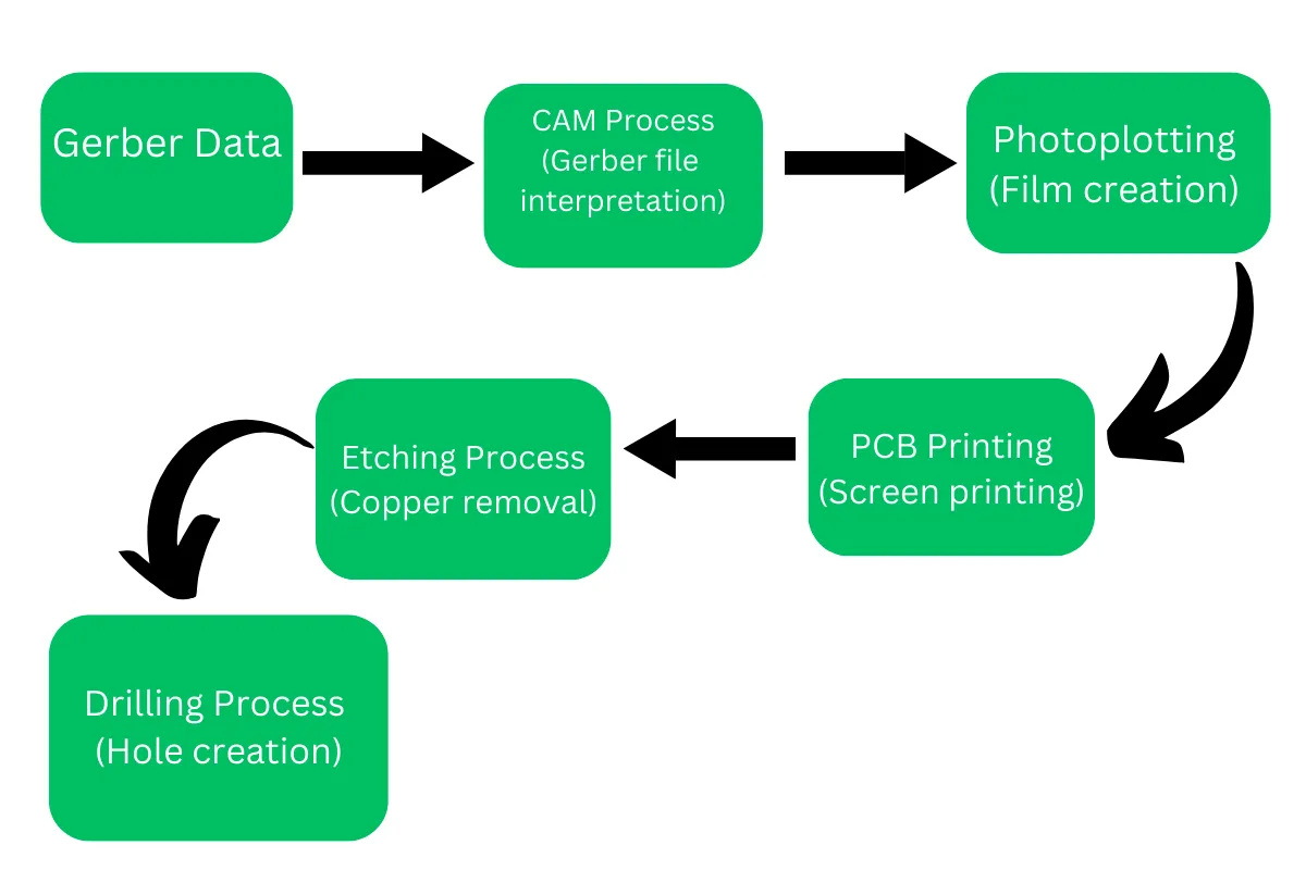
Design Validation
Before beginning the production process, manufacturers inspect the Gerber file. They search for design mistakes and possible problems. This is known as Design for Manufacturing (DFM). DFM provides the opportunity for manufacturers to rectify errors at an early stage. Rectifying these faults now will lead to saving both time and money in the future.
Photolithography
Files of Gerber are utilized in the process known as photolithography for making layers of film. Patterns on the board are formed by these films. The file instructs the machinery on where to make exposure to material that is sensitive to UV light. Once exposed, this material is developed, and copper traces are etched onto the board.
Drilling
Gerber files are important because they provide exact coordinates that help in drilling. It makes sure every hole is put at the right place. The holes that have been drilled play a crucial role in connecting different layers and putting components in their correct position. Without accurate drill data, the PCB will not function as intended.
Solder Mask Application
The layer of solder mask in Gerber files is used for stopping unnecessary connections. This layer covers places where there's no need for solder, lessening the chances of making solder bridges. Also, it safeguards copper lines from getting damaged while doing the process of soldering.
Silkscreen Printing
The layer of silkscreen includes labels and markings. It gives details such as where the components should be, their names, and numbers for reference. This supports assembling and checking PCBs with more ease. Gerber files specify the exact layout of these labels.
Check here to see the solder mask and silkscreen Capability of ALLPCB
Gerber File Formats and Compatibility with ALLPCB
The format of the Gerber file has undergone changes with time. The older versions had RS-274-D, but it had some restrictions. Nowadays, most people use the RS-274-X version. This style is also called the Extended Gerber format. People like RS-274-X as it brings together all necessary information in one file.
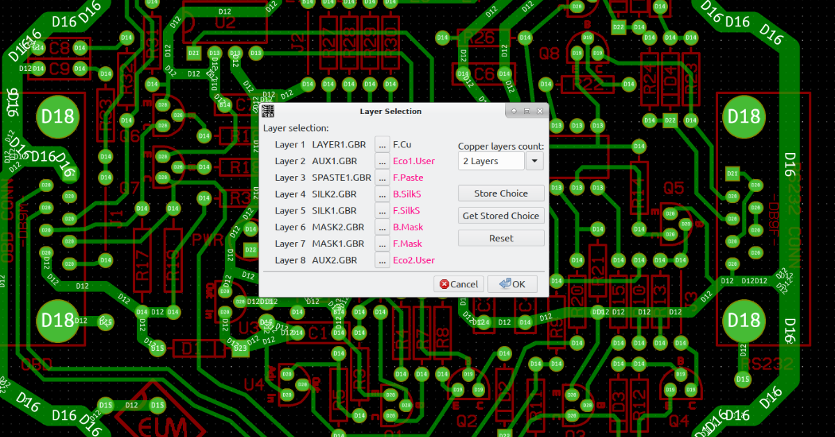
ALLPCB supports RS-274-X, which makes it a good option for those who design. The format lessens the probability of mistakes and accelerates the production process. All vital details like configurations, XY coordinates, apertures, and drawing commands are encompassed in RS-274-X.
Types of Gerber File Formats
-
RS-274-D
-
RS-274-X
-
Gerber X2
1. RS-274-D
RS-274-D is the initial format of Gerber. It was created during the beginning period of PCB design and has been extensively utilized for numerous years. This format was more straightforward and not as competent compared to subsequent versions.
RS-274-D is a simple structure that holds only crucial information. It gives coordinates for traces, pads, and other elements of the board.
But, RS-274-D does not contain built-in shape details. For defining shapes, it uses distinct aperture lists instead.
These lists for aperture are very important for the machine to comprehend the design. They communicate to the machine what forms (such as circles or rectangles) it needs to use and when in each characteristic.
Every hole has a unique size and shape, defined distinctly. To illustrate, one aperture may symbolize a 0.5 mm round pad, while another stands for a rectangular-shaped pad.
Due to the dependence on aperture lists, it is necessary to handle RS-274-D files with caution. If there's an absence or wrong interpretation of the aperture list, then it might lead to a misunderstanding of the design by the machinery.
RS-274-D was functional during its period, though it had restrictions. The task of handling different aperture lists consumed a lot of time. Additionally, it escalated the possibility of mistakes made by humans. As a result, more advanced formats were eventually developed.
2. RS-274-X
RS-274-X is the advanced form of the Gerber format. It emerged to tackle the restrictions found in RS-274-D. Rapidly, RS-274-X turned into the most popular Gerber format within the PCB sector.
All required data is combined into one file by RS-274-X. This encompasses coordinates, apertures and the settings parameters.
The requirement for distinct lists of apertures has been removed. Now, all the information about shape and size is incorporated directly into the file itself.
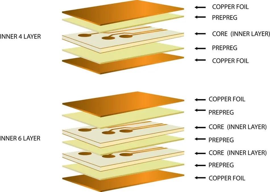
Every stratum in the PCB design is preserved as an individual RS-274-X file. As an illustration, the upper copper layer and the lower copper layer will possess their distinct files each.
The layout also contains setup options for higher accuracy. These configurations may define elements such as resolution and scaling.
Files of RS-274-X are simpler to handle as everything is included within them. This situation minimizes the possibility of mistakes that can happen due to absent or wrongly paired aperture lists.
The format known as RS-274-X accelerated and improved the accuracy of PCB design. The data structure was made simpler, which brought ease to both designers and manufacturers. Nowadays, the majority of companies manufacturing PCBs accept this RS-274-X format.
3. Gerber X2
Gerber X2 stands as the latest Gerber format that can be found. It was made to put more capabilities into RS-274-X. On top of all the features in RS-274-X, Gerber X2 brings more data too.
The files of Gerber X2 have functions of layers. Each file determines the type of layer it symbolizes; it could be copper, solder mask, or silkscreen.
Also, the layout contains characteristics of objects. These features give additional information, such as pad type or trace function.
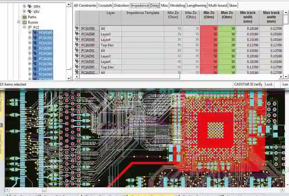
The Gerber X2 also has the ability to recognize traces controlled by impedance. This is beneficial for designs where maintaining signal integrity holds significant importance.
The fresh design further includes metadata for simplified handling of files. As an illustration, it can show the stack-up structure of PCBs.
Gerber X2 assists in enhanced data compatibility with sophisticated software. It enables designers to develop more intricate and detailed PCBs.
-
Copper layer identification without contact
-
Capability to clearly differentiate signal and power planes
-
Board layer characteristics, precise documentation
Another important benefit is improvement in accuracy. By design, X2 provides more robust information transfer between design software and manufacturing equipment. Such a structure avoids potential misunderstandings when the product is being produced.
-
Specific design intent notes
-
Manufacturing requirements
-
Component placement guidelines
-
Material specifications
Essential Elements in Gerber Files for PCB Production
In Gerber files, you will find several layers. Each one gives certain data for the production of PCB. These are the main layers in a Gerber file:
1. Copper Layers (Top and Bottom)
Layers of copper have traces and pads made from the same material. The layer at the top is where most elements are placed, while at the bottom, we find more connections, including those for ground planes. There's a separate Gerber file dedicated to each layer of copper.
2. Solder Mask Layers
The layers of the solder mask determine the regions that are coated by this material. This particular mask stops unwanted connections between traces and pads from being made by the solder. Both the top and bottom layers possess their own unique solder masks. These are critical for preventing short circuits.
3. Silkscreen Layers
Layers of silkscreen have labels, symbols, and identifiers included. These assist technicians and machines in recognizing components at the time of assembly. Silkscreen layers also display where each part is located and incorporate reference designators.
4. Drill Layer
The Dill Layer keeps data about locations for drilling holes. This layer shows exact spots to put each hole. Drills are used for making vias, which are connections between layers and also attaching components together.
5. Board Outline
The layer of board outline is what determines the physical form of the PCB. It holds significance in carving out the board with the right measurements. Furthermore, it provides assistance when integrating this board into enclosures.
Understanding Gerber File Extensions
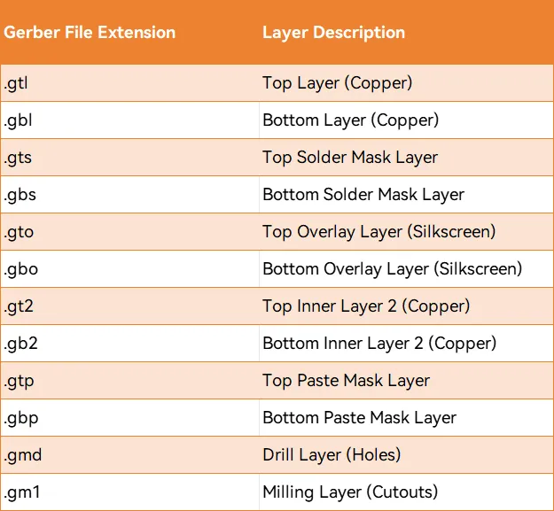
Every level in a Gerber file has a unique extension. These extensions convey the information to the PCB fabricators about their representing layer. Below is an enumeration of frequently seen Gerber file extensions:
-
GTL
-
GTS
-
GTO.
-
GBL
-
GBS
-
GBO
-
GTP
-
GBP
.GTL – Top Copper Layer
GTL is the abbreviation for the upper copper layer. This particular layer has copper traces on the top part of the PCB.
-
It includes all the electrical connections on the top side.
-
This layer holds the traces and pads where components are placed.
-
The top copper layer is essential for signal flow in the PCB.
.GTS – Top Solder Mask Layer
GTS is a representation of the uppermost layer of a solder mask. A protective covering over copper, that's what we call a solder mask.
-
This layer covers the top copper layer except for pads and vias.
-
It prevents the solder from bridging unwanted connections.
-
The solder mask also protects copper traces from environmental damage.
-
The .GTS file instructs the maker where to put the solder mask on the upper side.
.GTO – Top Silkscreen Layer
GTO is the superior layer of silkscreen. This level contains printed words and signs on the upper surface.
-
It shows labels for components, like resistors and capacitors.
-
Silkscreen helps in identifying parts during assembly.
-
The layer includes reference designators, outlines, and logos.
-
The .GTO file helps in determining where all the printed details should go on top of the PCB.
.GBL – Bottom Copper Layer
GBL is an abbreviation for the bottom copper layer. This layer accommodates the copper attachments on the lower side of PCB.
-
It includes all electrical paths and pads on the bottom side.
-
This layer is similar to the top copper layer but for the bottom.
-
It’s often used for ground planes or additional signal routing.
-
The .GBL file guides the maker in forming connections on the underside of the PCB.
.GBS – Bottom Solder Mask Layer
GBS represents the lower layer of the solder mask. It is there to safeguard copper pathways on its underneath side.
-
The solder mask covers all copper areas except exposed pads.
-
This layer prevents the solder from accidentally connecting traces.
-
It also protects the copper from moisture and contaminants.
The .GBS file determines the location to put the solder mask on the lower part of the board.
.GBO – Bottom Silkscreen Layer
-
It includes labels for components that are on the bottom.
-
Silkscreen helps with part identification during assembly.
-
This layer often includes mirrored text to align with top-side markings.
The .GBO file assists the producer in appending printed data on the lower part of the PCB.
.GTP – Top Paste Layer
GTP is the abbreviation for top paste layer. This specific layer has application in the Assembly of Surface Mount Technology (SMT).
-
It shows where solder paste should be applied on the top side.
-
The solder paste helps mount components to the board.
-
This layer aligns with the pads on the top copper layer.
The .GTP file helps to direct the template which applies solder paste for SMT components on above.
.GBP – Bottom Paste Layer
.GBP represents the bottom paste layer. This layer is also used for SMT assembly.
-
It shows where the solder paste should go on the bottom side.
-
The paste layer is necessary if components are mounted on both sides.
-
It aligns with the pads on the bottom copper layer.
The .GBP file assists in making the stencil for applying solder paste on the bottom side.
How to Generate Gerber Files Using Different Software?
You need PCB design software to create Gerber files. Here are steps to create Gerber files in Altium Designer, KiCad, Eagle, and EasEDA.
Altium Designer
-
Open the PCB layout in Altium Designer.
-
Click on File > Fabrication Outputs > Gerber Files.
-
Set RS-274-X as the output format.
-
Select layers ( copper, solder mask, and silkscreen.)
-
Click OK to export the Gerber files.
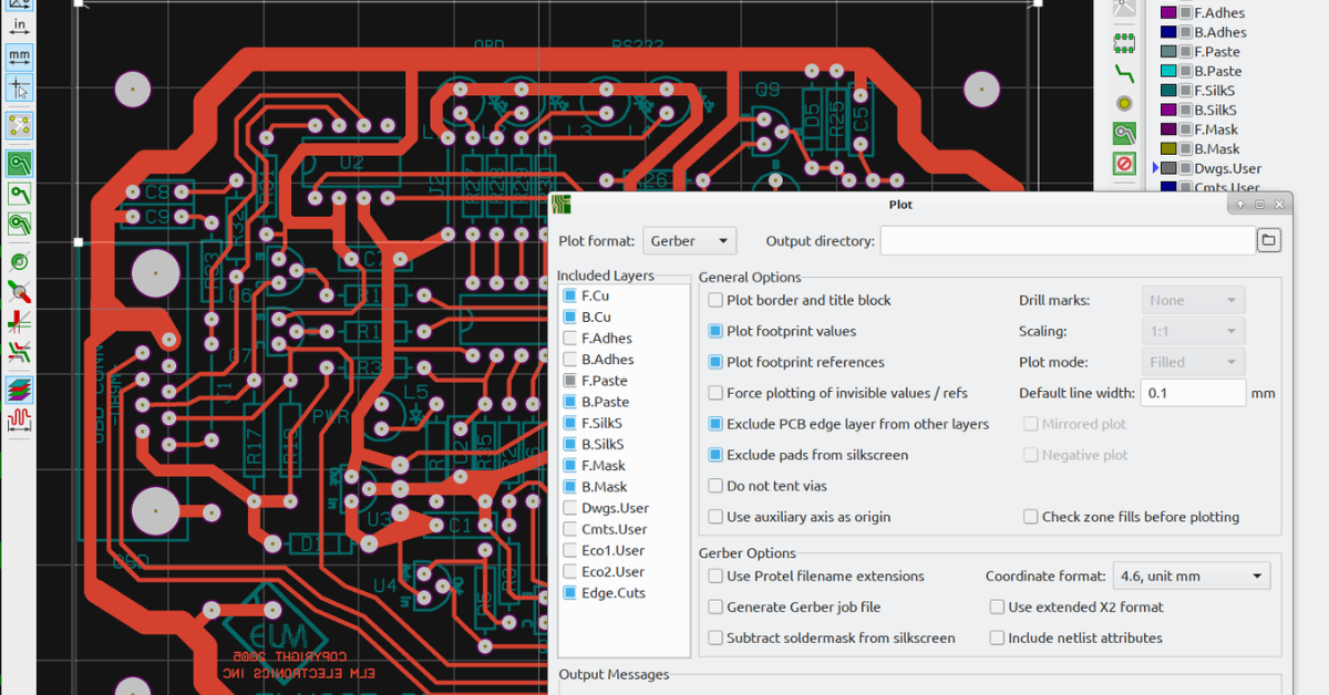
KiCad
-
Open the PCB project in KiCad.
-
Go to File > Plot.
-
Choose RS-274-X as the plot format.
-
Select required layers like copper, mask, and drill.
-
Click Plot to generate Gerber files.
Eagle
-
Open the PCB layout in Eagle.
-
Choose CAM Processor from the File menu.
-
Select RS-274-X as the output format.
-
Specify the layers to export, such as top copper, bottom copper, and drill.
-
Click Process Job to create the Gerber files.
EasyEDA
-
Open your project in EasyEDA.
-
Select Fabrication > PCB Fabrication File (Gerber).
-
Choose the layers and other important settings.
-
Click Generate Gerber to export.
Viewing and Verifying Gerber Files
-
Gerbv: Open-source viewer.
-
ViewMate: Advanced viewer with editing options.
-
ZofzPCB: Viewer with 3D visualization.
-
Eurocircuits: Cloud-based viewer.
Each viewer has features for inspecting layers and checking alignment. Verifying files helps prevent mistakes in the final PCB.
Gerber File Optimization
Modern PCB design workflows require file size management. However, large Gerber files can be a big problem during data transfer and processing.
-
Layer Merging Strategies:
-
Combine redundant layers
-
Remove unnecessary whitespace
-
Get rid of duplicate geometric information
-
Your data should use efficient compression algorithms.
-
Choose the right file formats.
-
Use as few graphic elements as possible.
These techniques guarantee faster file transfers and more efficient manufacturing processes. You can shrink file sizes 30-50% without losing critical design information using professional designers.
Gerber File Security
-
Digital watermarking
-
Encryption techniques
-
Distribution protocols limited
-
Access control mechanisms
Tips for Preparing and Submitting Gerber Files for Manufacturing
-
Check All Layers: Check all necessary layers are included.
-
Use Standard Naming: Standard layer names help avoid confusion.
-
Compress Files: Incorporate a compressed folder to simplify upload.
Conclusion
Gerber files serve as the base for the manufacturing of PCB. They give exact directions for each layer of PCB. By employing suitable software for designing your PCB and abiding by optimal methods, Gerber files that align with industry measures can be developed. When you check files with a viewer, it decreases the chance of mistakes and guarantees an effective production run.


