 ALLPCB


In the world of PCB design, via filling is a critical process that can significantly impact the performance, reliability, and durability of your circuit board. Whether you're working on high-density interconnect (HDI) designs or multilayer boards, understanding via filling techniques and materials is essential. This guide dives deep into the essentials of via filling, covering via filling materials, conductive via fill, non-conductive via fill, epoxy via fill, and via plugging. If you're looking to optimize your PCB design for better electrical conductivity, thermal management, or structural integrity, you've come to the right place.
At its core, via filling is the process of filling the tiny holes (vias) in a PCB that connect different layers of the board. These vias can be filled with conductive or non-conductive materials to achieve specific design goals. In this comprehensive guide, we'll break down the types of via filling, their benefits, and how to choose the right approach for your project.
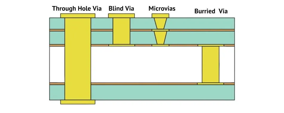
What Is Via Filling in PCB Design?
Vias are small holes drilled into a printed circuit board (PCB) to create electrical connections between different layers. Without vias, signals and power cannot travel between the layers of a multilayer board. However, leaving these holes empty can lead to issues like weak structural integrity, poor thermal dissipation, or solder wicking during assembly. Via filling addresses these problems by filling the vias with specific materials, ensuring better performance and reliability.
Via filling serves multiple purposes depending on the material used. It can enhance electrical conductivity for high-speed signals, improve heat dissipation in high-power applications, or simply provide mechanical strength to prevent cracks or damage. With modern PCB designs becoming more complex, especially in HDI PCBs, via filling has become a standard practice to meet tight tolerances and high-performance demands.
Why Is Via Filling Important?
Via filling plays a vital role in modern PCB fabrication. Here are some key reasons why it matters:
- Improved Electrical Performance: Filling vias with conductive materials can reduce impedance and improve signal integrity, especially for high-frequency applications where signal loss must be minimized. For instance, in a high-speed design operating at 5 GHz, a filled via can help maintain signal integrity by reducing parasitic capacitance.
- Better Thermal Management: Conductive fills, like copper, can transfer heat away from components, preventing overheating in high-power designs. This is critical for applications like LED lighting or power supplies where thermal dissipation is a priority.
- Enhanced Structural Integrity: Filling vias adds mechanical strength to the board, reducing the risk of cracks or delamination during manufacturing or operation.
- Prevention of Solder Wicking: Non-conductive via fill materials prevent solder from flowing into vias during assembly, avoiding issues like short circuits or uneven solder joints.
Types of Via Filling Materials
Choosing the right via filling material is crucial for achieving your design goals. Below, we explore the most common via filling materials used in PCB design, focusing on their properties and applications.
1. Conductive Via Fill Materials
Conductive via fill materials are used when electrical connectivity or thermal dissipation is a priority. These materials create a solid conductive path through the via, enhancing signal transmission and heat transfer.
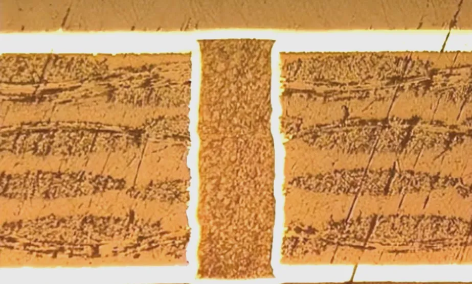
- Copper Fill: Copper is the most common conductive material for via filling. It offers excellent electrical conductivity (approximately 5.96 x 10^7 S/m) and thermal conductivity (401 W/m·K), making it ideal for high-speed and high-power applications. Copper-filled vias are often used in HDI designs to support stacked vias and ensure reliable interlayer connections.
- Silver Epoxy: Silver-based conductive epoxy is another option, offering good conductivity and ease of application. It’s often used in applications where copper plating isn’t feasible, though it’s less common due to higher costs.
Conductive via fill is perfect for designs requiring minimal signal loss or high current capacity. However, it can be more expensive and complex to implement compared to non-conductive options.
2. Non-Conductive Via Fill Materials
Non-conductive via fill materials are used primarily for structural support and to prevent solder wicking. They don’t contribute to electrical conductivity but are essential for certain design needs.
- Epoxy Via Fill: Epoxy-based materials are widely used for non-conductive via filling. They provide excellent mechanical strength and are resistant to thermal stress, making them suitable for vias under components or in high-density areas. Epoxy via fill also helps create a flat surface for better soldering during assembly.
- Polymer Fill: Polymers are another non-conductive option, often chosen for their low cost and ease of processing. They’re ideal for less demanding applications where structural support is the main concern.
Non-conductive via fill is often more cost-effective than conductive fill and is commonly used in standard multilayer boards to improve reliability without adding electrical connections.
Conductive Via Fill vs. Non-Conductive Via Fill: Which to Choose?
Deciding between conductive and non-conductive via fill depends on your specific design requirements. Let’s break down the key differences and use cases:
- Conductive Via Fill:
- Best For: High-speed designs, high-power applications, and HDI boards where signal integrity and thermal management are critical.
- Advantages: Reduces impedance (e.g., lowering via impedance from 50 ohms to 45 ohms in some designs), improves heat dissipation, and supports stacked vias.
- Disadvantages: Higher cost and more complex manufacturing process.
- Non-Conductive Via Fill:
- Best For: Standard multilayer boards, designs requiring structural support, or to prevent solder wicking during assembly.
- Advantages: Cost-effective, simpler to implement, and provides a flat surface for soldering.
- Disadvantages: No contribution to electrical or thermal performance.
For example, if you’re designing a high-frequency board for 5G applications, conductive via fill with copper would be the better choice to maintain signal integrity. On the other hand, for a simple consumer electronics board, non-conductive epoxy via fill might suffice to ensure structural integrity and ease of assembly.
Via Plugging: An Alternative to Via Filling
Via plugging is a related but distinct process from via filling. While via filling completely fills the via with material, via plugging typically involves partially filling or capping the via to protect it during manufacturing or assembly. Plugging is often done with non-conductive materials like epoxy to prevent solder or contaminants from entering the via.
Via plugging is commonly used in designs with vias near surface-mount components. It prevents solder paste from flowing into the via during reflow soldering, which could cause uneven joints or shorts. Unlike full via filling, plugging doesn’t necessarily add significant mechanical strength or conductivity but serves as a protective measure.
Key Benefits of Via Plugging:
- Protects vias from solder wicking during assembly.
- Ensures a cleaner and more reliable soldering process.
- Cost-effective for designs that don’t require full via filling.
Suggested Reading: Through-Hole Via Filling and Plugging: When and Why
Epoxy Via Fill: A Popular Choice for Non-Conductive Filling
Epoxy via fill is one of the most widely used non-conductive filling methods due to its versatility and reliability. Epoxy materials are specially formulated to withstand the thermal and mechanical stresses of PCB manufacturing and operation. They’re applied to vias using techniques like screen printing or vacuum filling, ensuring a complete and uniform fill.
Advantages of Epoxy Via Fill:
- Provides a smooth, flat surface for better component placement and soldering.
- Enhances the structural integrity of the board, reducing the risk of cracks under thermal stress (e.g., during reflow soldering at 260°C).
- Prevents air pockets or voids in vias, which could lead to reliability issues over time.
Epoxy via fill is especially useful in HDI designs where vias are placed under components like ball grid arrays (BGAs). By filling these vias, you ensure that the surface remains even, allowing for proper soldering and reducing the risk of defects.
Techniques for Via Filling in PCB Fabrication
The process of via filling can vary depending on the material and design requirements. Here are some common techniques used in PCB manufacturing:
- Screen Printing: A stencil or screen is used to apply epoxy or other materials into the vias. This method is cost-effective for non-conductive fills and works well for larger vias.
- Vacuum Filling: For smaller vias or high-density designs, vacuum filling ensures that the material completely fills the via without air pockets. This technique is often used for epoxy via fill in HDI boards.
- Electroplating for Conductive Fill: Copper via filling is typically done through electroplating, where copper is deposited into the via to create a solid conductive path. This method is precise but requires additional manufacturing steps.
Each technique has its trade-offs in terms of cost, precision, and suitability for specific via sizes. For instance, vacuum filling is ideal for vias smaller than 0.3 mm, while screen printing may suffice for larger vias above 0.5 mm.
Best Practices for Via Filling in PCB Design
To ensure the best results from via filling, consider the following best practices during the design and fabrication stages:
- Define Via Filling Requirements Early: Specify whether you need conductive or non-conductive fill in your design files. Clear documentation helps avoid miscommunication with your manufacturer.
- Choose the Right Material: Match the via filling material to your design needs. For high-speed signals, opt for conductive copper fill; for cost-effective structural support, choose epoxy via fill.
- Consider Via Size and Aspect Ratio: Smaller vias or those with high aspect ratios (depth-to-diameter) may require advanced filling techniques like vacuum filling to avoid voids.
- Test for Reliability: After fabrication, perform thermal cycling and electrical testing to ensure that filled vias meet performance expectations. For example, test for thermal resistance in high-power designs to confirm heat dissipation.
Challenges and Limitations of Via Filling
While via filling offers numerous benefits, it’s not without challenges. Understanding these limitations can help you make informed decisions:
- Cost: Conductive via filling, especially with copper, can significantly increase manufacturing costs, particularly for large boards with many vias.
- Manufacturing Complexity: Filling small vias or achieving uniform fills in high-density designs requires advanced equipment and expertise, which may not be available with all manufacturers.
- Thermal Expansion: Some via filling materials, like epoxy, have different coefficients of thermal expansion (CTE) compared to the PCB substrate. This mismatch can lead to stress or cracks during thermal cycling (e.g., CTE of epoxy at 50 ppm/°C vs. FR4 at 14 ppm/°C).
To mitigate these challenges, work closely with your fabrication partner to select materials and processes that balance cost, performance, and reliability.
Conclusion: Optimizing Your PCB with Via Filling
Via filling is a powerful technique to enhance the performance, reliability, and manufacturability of your PCB designs. Whether you choose conductive via fill for high-speed signals, non-conductive epoxy via fill for structural support, or via plugging to protect against solder wicking, understanding the options and their applications is key to success. By carefully selecting via filling materials and techniques, you can address the unique challenges of your design and achieve optimal results.
From improving signal integrity to ensuring thermal management, via filling offers solutions for a wide range of PCB design needs. As designs continue to push the boundaries of density and complexity, mastering via filling will remain a critical skill for engineers and designers. With this guide, you’re equipped with the knowledge to make informed decisions and create high-performing, reliable circuit boards.


