In modern electronic design, signal integrity has become one of the most critical factors influencing system performance, particularly in high-speed and high-frequency applications. A key element in maintaining signal integrity is the printed circuit board stack-up design. The stack-up not only determines the electrical performance of the board but also affects manufacturability, cost, thermal performance, and electromagnetic compatibility (EMC).
What Is a PCB Stack-Up?
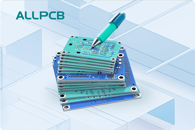
A PCB stack-up refers to the arrangement of copper layers and insulating dielectric materials in a multi-layer PCB. It outlines how the layers are positioned—signal, power, ground—and their order, thickness, and material composition. Typical stack-ups include 4, 6, 8, or more layers, depending on the complexity of the design.
A well-planned stack-up helps reduce noise, manage impedance, control crosstalk, and ensure robust power distribution. As such, stack-up design must be considered early in the PCB layout process and not treated as an afterthought.
Key Components of Stack-Up Design
1. Layer Types
- Signal Layers: Carry digital or analog signals.
- Power/Ground Planes: Provide power distribution and return paths for signal currents.
- Dielectric Layers: Insulating materials between copper layers, typically made from FR-4, Rogers, or other specialty laminates.
2. Symmetry and Balance
A balanced stack-up prevents warping during manufacturing and helps maintain uniform mechanical and thermal properties. Symmetry in the placement of copper layers and dielectric thickness is often required.
3. Impedance Control
Characteristic impedance is determined by trace width, dielectric height, and dielectric constant. Controlled impedance is essential for maintaining signal integrity, especially for high-speed interfaces like DDR, USB, and PCIe.
How Stack-Up Affects Signal Integrity
1. Impedance Matching
A mismatch in impedance causes reflections that can corrupt signal transmission. Proper stack-up design enables designers to model and maintain consistent impedance across traces.
For example, a microstrip line (a trace on an outer layer with a reference ground plane underneath) has a different impedance than a stripline (a trace sandwiched between two ground planes). Understanding these differences helps in routing high-speed signals correctly.
2. Minimizing Crosstalk
Crosstalk occurs when signals on adjacent traces interfere with each other. A well-designed stack-up can reduce crosstalk by:
- Increasing spacing between signal layers
- Using ground planes as isolation buffers
- Keeping high-speed signal layers adjacent to continuous ground planes
3. Return Path Integrity
Signal currents return to the source via the path of least inductance. In stack-up design, placing a solid reference plane (ground) next to signal layers ensures a short, uninterrupted return path, minimizing loop area and EMI.
4. Power Integrity
A low-impedance power distribution network (PDN) is critical for stable operation. Power and ground planes form a parallel plate capacitor, offering high-frequency decoupling and reducing noise. Using multiple planes and proper stack-up arrangements can enhance power integrity.
Common Stack-Up Configurations
4-Layer PCB
- Top Layer: Signal
- Layer 2: Ground
- Layer 3: Power
- Bottom Layer: Signal
This configuration provides basic impedance control and is cost-effective. However, signal layers are further apart, which may increase crosstalk and EMI.
6-Layer PCB
- Top Layer: Signal
- Layer 2: Ground
- Layer 3: Signal
- Layer 4: Signal
- Layer 5: Power
- Bottom Layer: Signal
Better suited for higher speed applications with improved isolation and power distribution.
8-Layer PCB
Provides excellent signal integrity, EMI performance, and power integrity. Recommended for complex designs like high-speed networking and processor boards.
Material Considerations
The choice of dielectric material affects the dielectric constant (Dk) and loss tangent (Df), which impact signal speed and attenuation. For example:
FR-4: Common and cost-effective, but limited performance above 1 GHz
Rogers: Low Dk/Df, better for RF and high-speed digital
Polyimide: High-temperature applications
Choosing the right material is essential for maintaining signal integrity, especially in high-frequency designs.
Tools and Simulation
Advanced EDA tools like Altium Designer, Cadence Allegro, or Mentor PADS offer stack-up configuration and impedance modeling. Designers should simulate signal integrity using tools like HyperLynx or Ansys SIwave before finalizing the layout.
Best Practices for Stack-Up Design
1. Always place high-speed signals adjacent to a continuous ground plane.
2. Keep differential pairs on the same layer and maintain consistent spacing.
3. Avoid unnecessary layer transitions (vias) for high-speed nets.
4. Use simulation to validate impedance, crosstalk, and timing.
5. Ensure symmetrical stack-up to prevent warpage.
Conclusion
PCB stack-up design plays a vital role in the electrical performance and reliability of electronic systems. As signal speeds increase, so do the demands on stack-up precision and planning. By understanding the principles of stack-up design and its impact on signal integrity, designers can build PCBs that are robust, efficient, and ready for the next generation of high-speed technology.
 ALLPCB


