 ALLPCB


If you're an electrical engineer working on electric vehicle (EV) battery management systems (BMS), you might be wondering how to optimize your PCB layout for high-voltage connectors. The answer lies in careful planning around connector placement, insulation coordination, arc suppression, and safety interlocks to ensure reliability and safety. In this blog, we'll dive deep into the specifics of high voltage PCB layout, offering actionable tips and detailed strategies to help you design robust systems for automotive applications. Let's explore how to tackle challenges like partial discharge and ensure your design meets the stringent demands of EV technology.
Why High-Voltage PCB Layout Matters in EV Battery Management Systems
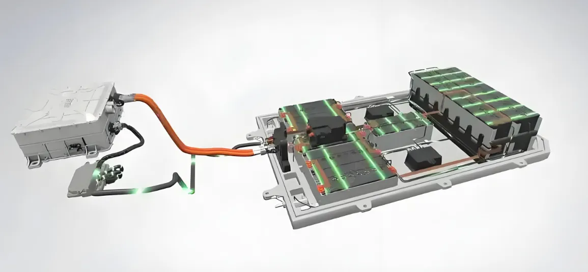
Electric vehicles rely on battery management systems to monitor and control high-voltage battery packs, often operating at voltages between 400V and 800V. A poorly designed high voltage PCB layout can lead to catastrophic failures like electrical arcing, insulation breakdown, or even fires. For engineers, optimizing the PCB layout isn't just about performance—it's about safety and compliance with automotive standards like ISO 26262.
In this post, we'll cover key aspects of designing a PCB for EV BMS, focusing on connector placement, arc suppression techniques, and other critical factors. Whether you're new to EV design or a seasoned engineer, these insights will help you create safer, more efficient systems.
Key Challenges in High-Voltage PCB Design for EV BMS
Before diving into solutions, let's understand the unique challenges of designing a PCB for high-voltage applications in EVs:
- Voltage Stress: Voltages up to 800V can cause partial discharge or dielectric breakdown if traces and components aren't properly spaced.
- Thermal Management: High currents (often exceeding 100A) generate heat, which can degrade insulation and components.
- Electromagnetic Interference (EMI): Rapid switching in BMS circuits can interfere with sensitive signals if not mitigated.
- Safety Risks: Without proper insulation coordination and safety interlocks, there's a risk of electric shock or system failure.
Addressing these challenges requires a systematic approach to PCB design, starting with the placement of high-voltage connectors.
Best Practices for Connector Placement in High-Voltage PCBs
Connector placement is a critical first step in optimizing a high-voltage PCB layout. Poorly placed automotive connectors can lead to voltage creep, arcing, and signal interference. Here are some practical tips:
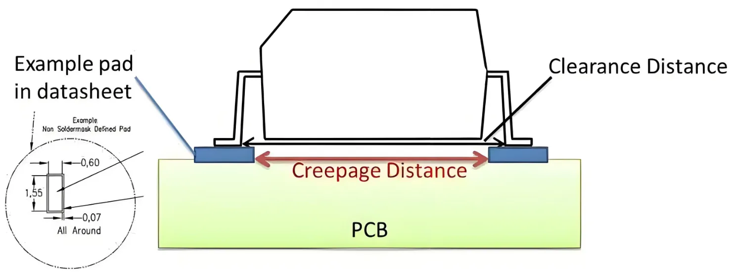
- Maximize Clearance and Creepage Distances: For a system operating at 800V, maintain a clearance (air gap) of at least 8mm and a creepage distance (surface path) of 10mm between high-voltage traces and connectors, as per IEC 60664-1 standards. This reduces the risk of arcing and partial discharge.
- Position Connectors Near Edges: Place high-voltage connectors near the PCB edge to minimize trace lengths and reduce the risk of interference with other circuits. This also makes it easier to implement shielding.
- Group by Voltage Levels: Separate high-voltage connectors (e.g., battery input/output) from low-voltage ones (e.g., communication lines) to avoid cross-talk and ensure proper insulation coordination.
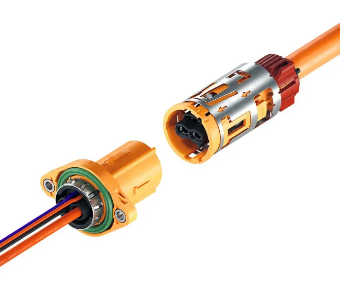
- Use Robust Automotive Connectors: Opt for connectors rated for high-voltage and high-current applications, such as TE Connectivity's AMP+ series, which can handle up to 1000V and 200A, ensuring reliability in harsh automotive environments.
Arc Suppression Techniques for High-Voltage PCBs
Electrical arcing is a significant concern in EV BMS designs due to the high voltages involved. Arc suppression techniques are essential to prevent damage and ensure safety. Here's how to mitigate this risk:
- Use Dielectric Barriers: Incorporate insulating materials like FR-4 with a high dielectric strength (around 20kV/mm) between high-voltage traces and connectors to prevent arc formation.
- Implement Conformal Coating: Apply a conformal coating with a dielectric strength of at least 500V/mil to the PCB surface. This protects against moisture and dust, which can trigger arcing, especially in humid automotive environments.
- Design for Overvoltage Protection: Include transient voltage suppressors (TVS diodes) near high-voltage connectors to clamp voltage spikes, which could otherwise cause arcing. For example, a TVS diode rated for 1000V can protect against surges in an 800V system.
- Optimize Trace Geometry: Avoid sharp corners on high-voltage traces, as they can concentrate electric fields and increase the likelihood of arcing. Use rounded corners with a minimum radius of 0.5mm.
By combining these techniques, you can significantly reduce the risk of arcing, enhancing the reliability of your BMS design.
Insulation Coordination: A Must for Safety
Insulation coordination ensures that all parts of your high-voltage PCB can withstand the electrical stresses they encounter. This is especially critical in EV BMS, where a failure could endanger lives. Follow these guidelines:
- Select Appropriate Materials: Use PCB substrates with high comparative tracking index (CTI) values, such as FR-4 with a CTI of 600, to resist surface breakdown under high voltage.
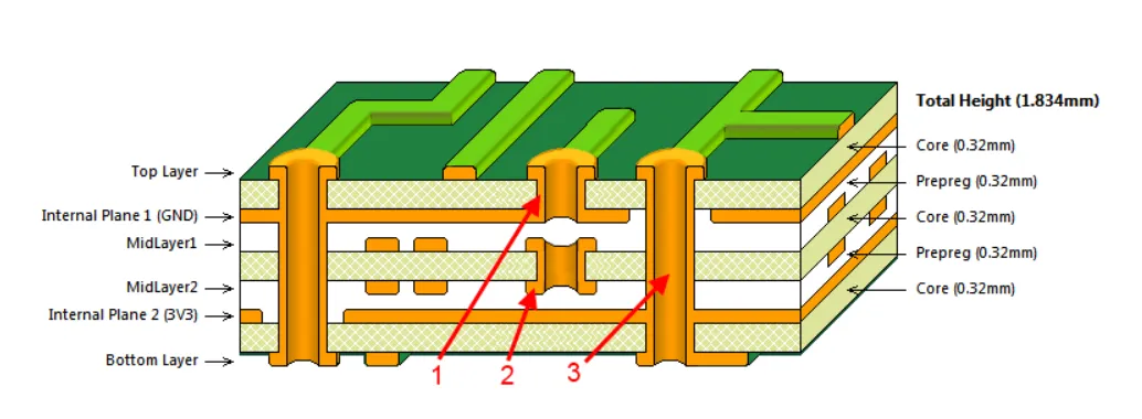
- Layer Stacking for Isolation: In multilayer PCBs, dedicate specific layers to high-voltage traces and separate them from low-voltage signals with ground planes. A typical stack-up might include a 1.6mm thick board with at least 0.2mm dielectric spacing between layers.
- Test for Dielectric Strength: After design, subject your PCB to hipot testing at 1.5 times the operating voltage (e.g., 1200V for an 800V system) to verify insulation integrity.
Implementing Safety Interlocks in High-Voltage Designs
Safety interlocks are non-negotiable in EV BMS to protect users and technicians from high-voltage hazards. These systems ensure that power is disconnected during maintenance or in fault conditions. Here's how to integrate them into your PCB layout:
- Design for High-Voltage Disconnect: Include a high-voltage interlock loop (HVIL) circuit near connectors. This loop uses low-voltage signals (typically 5V or 12V) to detect if a connector is disconnected, triggering a shutdown of the high-voltage system.
- Place Interlock Circuits Strategically: Position HVIL components close to high-voltage connectors to minimize latency in fault detection. Ensure traces for interlock signals are shielded to prevent EMI interference.
- Redundancy for Reliability: Use dual interlock circuits for critical connectors to provide redundancy. If one fails, the other can still trigger a shutdown, meeting automotive safety standards.
Implementing robust interlocks not only enhances safety but also builds trust in your BMS design among manufacturers and end-users.
Mitigating Partial Discharge in High-Voltage PCBs
Partial discharge (PD) occurs when small electrical discharges happen within insulation or at interfaces, gradually degrading materials and leading to failure. For EV BMS operating at high voltages, PD is a silent killer. Here's how to address it:
- Smooth Electric Field Distribution: Avoid sharp edges or points on conductors, as they create high electric field concentrations prone to PD. Use field grading techniques, such as adding guard rings around high-voltage pads.
- High-Quality Insulation: Choose insulation materials with low void content to prevent internal discharges. For example, use epoxy-based coatings with a breakdown strength of over 30kV/mm.
- Monitor and Test: During prototyping, use PD detection equipment to identify hotspots on your PCB under operating conditions (e.g., 800V at 85°C). Address any detected discharges by increasing spacing or improving insulation.
By proactively managing PD, you can extend the lifespan of your BMS and prevent unexpected failures in the field.
Choosing the Right Automotive Connectors for EV BMS
The choice of automotive connectors directly impacts the performance and safety of your high-voltage PCB. Here are key considerations for selecting connectors:
- Voltage and Current Ratings: Ensure connectors are rated above your system's maximum, e.g., a 1000V/150A connector for an 800V/100A BMS, to provide a safety margin.
- Environmental Resistance: Automotive connectors must withstand vibration, temperature swings (-40°C to 125°C), and humidity. Look for IP67-rated connectors like those from Amphenol or Molex.
- Shielding for EMI: Use connectors with built-in shielding to reduce EMI, especially for high-voltage lines near sensitive BMS circuits.
Practical Tips for Finalizing Your High-Voltage PCB Design
Once you've addressed connector placement, arc suppression, and safety features, follow these final steps to ensure your design is ready for production:
- Simulate Before Prototyping: Use tools like Altium Designer or Cadence to simulate electric field distribution and thermal performance. For instance, ensure no hotspot exceeds 125°C under a 100A load.
- Adhere to Standards: Follow automotive standards like AEC-Q100 for component reliability and ISO 16750 for environmental testing to ensure your design meets industry expectations.
- Iterate Based on Testing: After building a prototype, conduct high-voltage stress tests and thermal imaging to identify weaknesses. Adjust trace widths (e.g., increase from 2mm to 3mm for high-current paths) or spacing as needed.
Conclusion: Building Safer, More Reliable EV BMS with Optimized PCB Layouts
Designing a high voltage PCB layout for EV battery management systems is no small task. By focusing on connector placement, arc suppression, partial discharge mitigation, insulation coordination, and safety interlocks, you can create a system that’s both efficient and safe. The right automotive connectors and adherence to standards further ensure reliability in the demanding conditions of electric vehicles.
As an engineer, your goal is to balance performance with safety. Use the tips and strategies in this guide to refine your designs, simulate rigorously, and test thoroughly. By applying these principles, you're not just designing a PCB—you're contributing to the future of sustainable transportation. Let's keep pushing the boundaries of EV technology together!


