 ALLPCB


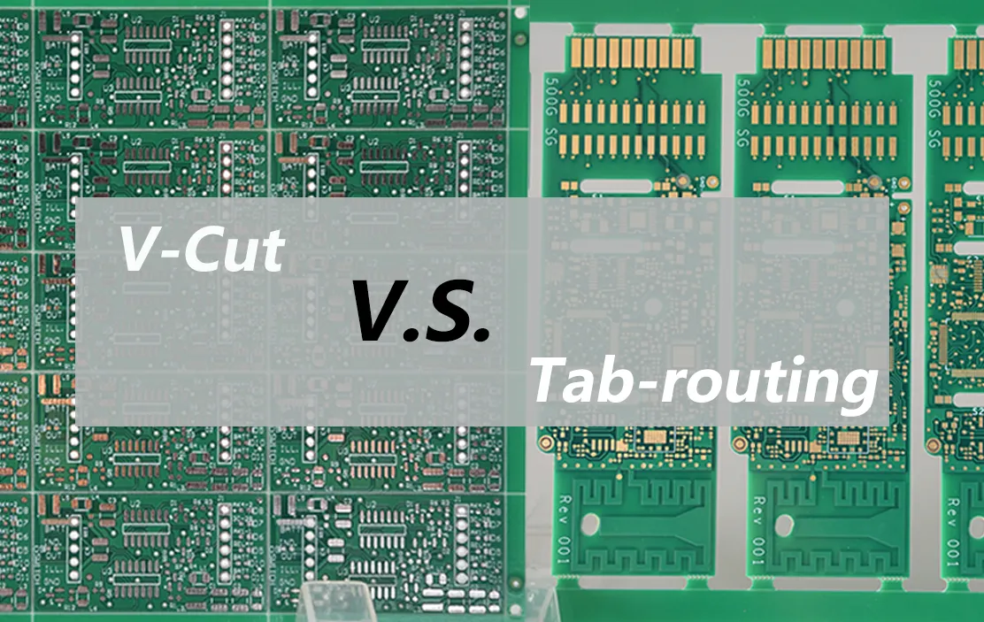
If you're searching for ways to achieve clean PCB depaneling and stress-free PCB depaneling, mastering tab routing is the key. This technique allows you to separate individual printed circuit boards (PCBs) from a larger panel with precision, minimizing stress on components and ensuring high-quality results. In this comprehensive guide, we'll explore effective PCB tab routing strategies and advanced PCB design tips to help you streamline the depaneling process. Whether you're a seasoned engineer or new to PCB manufacturing, you'll find practical insights to improve your workflow.
What Is Tab Routing and Why Does It Matter for PCB Depaneling?
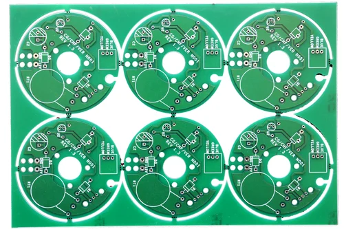
Tab routing is a widely used method in PCB manufacturing to separate individual boards from a panel. During production, multiple PCBs are often fabricated together on a single panel to save time and reduce costs. Once manufacturing is complete, these boards need to be separated, or "depanelized," without damaging the delicate components or traces. Tab routing involves creating small, breakable tabs (also called break tabs or mouse bites) that hold the boards together during production but allow for easy separation afterward.
The importance of tab routing lies in its ability to balance strength and ease of separation. Properly designed tabs keep the panel intact during assembly processes like soldering, yet they break cleanly without causing stress to the board or components. Poorly designed tabs, on the other hand, can lead to jagged edges, microcracks, or even damaged circuits. By mastering tab routing, you ensure clean PCB depaneling and maintain the integrity of your design—key goals for any advanced PCB design project.
Benefits of Stress-Free PCB Depaneling with Tab Routing
Using tab routing for stress-free PCB depaneling offers several advantages, especially for high-precision or complex designs. Here are some key benefits:
- Reduced Mechanical Stress: Unlike methods like manual breaking or shearing, tab routing minimizes physical stress on the board, protecting sensitive components and thin traces.
- Cost-Effective Production: Tab routing is compatible with automated manufacturing processes, reducing labor costs and time compared to more manual depaneling methods.
- Cleaner Edges: When designed correctly, tabs break off smoothly, leaving minimal residue or rough edges that could affect the board's appearance or functionality.
- Flexibility in Design: Tab routing works well for irregular board shapes and complex layouts, making it ideal for advanced PCB design applications.
By focusing on stress-free techniques, you can avoid common issues like delamination or component failure, ensuring your boards meet strict quality standards.
Key Techniques for Clean PCB Depaneling Using Tab Routing
Achieving clean PCB depaneling requires careful planning and execution. Below are proven techniques to optimize your tab routing process for the best results.
1. Optimize Tab Placement for Minimal Stress
The placement of break tabs is critical to reducing stress during depaneling. Tabs should be positioned in areas of the board that are away from sensitive components or high-density trace regions. Ideally, place tabs along the edges of the board where there is less risk of damaging critical circuitry. A common guideline is to space tabs evenly, with at least two to three tabs per side for smaller boards (e.g., under 50mm x 50mm) and more for larger ones.
For example, on a 100mm x 100mm board, placing five tabs per side—spaced approximately 20mm apart—provides stability during assembly while allowing for easy separation. Avoid placing tabs near corners, as this can create stress points that lead to cracks during depaneling.
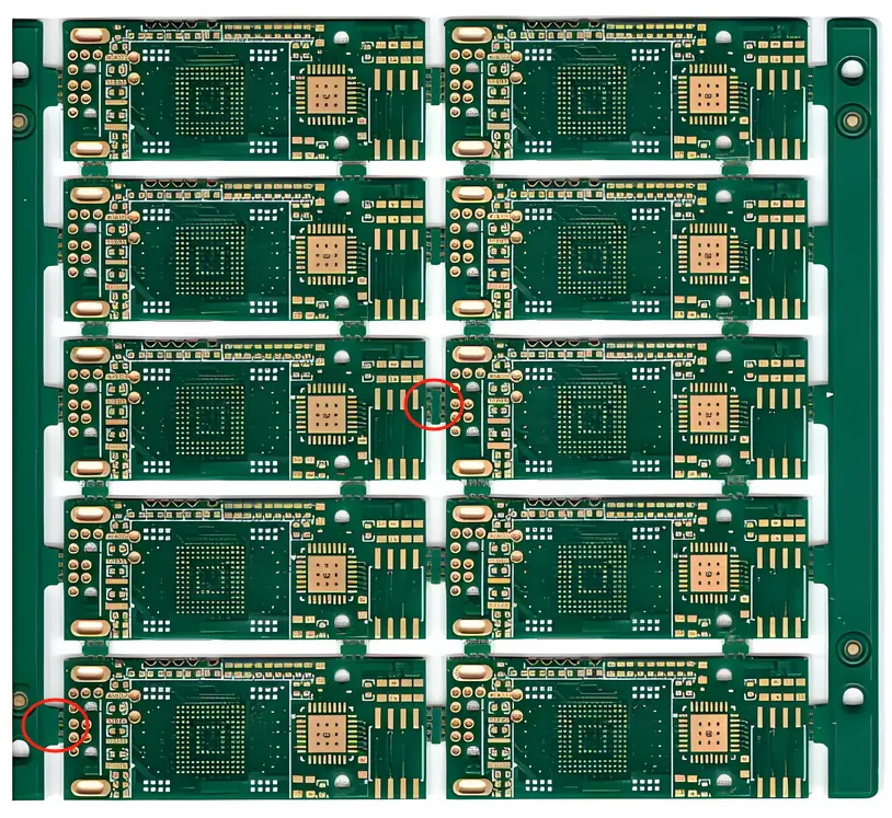
2. Use Mouse Bites for Smooth Breakage
Mouse bites are small, perforated holes drilled into the tabs to weaken them for easy separation. This technique is essential for clean PCB depaneling, as it ensures the tab breaks at the intended point without excessive force. A typical mouse bite pattern consists of 5 to 7 small holes (0.3mm to 0.5mm in diameter) spaced closely together within a 1mm to 2mm tab width.
The key is to balance the number and size of holes. Too few holes make the tab too strong, requiring more force to break and risking stress on the board. Too many holes can weaken the tab excessively, causing it to break prematurely during assembly. Testing different patterns during the prototyping phase can help you find the right configuration for your design.
3. Choose the Right Tab Width and Thickness
Tab dimensions directly impact the ease of depaneling and the structural integrity of the panel during production. A common tab width is between 1.5mm and 3mm, depending on the board's size and weight. Thicker boards (e.g., 2.0mm or more) may require wider tabs to withstand handling stress, while thinner boards (e.g., 0.8mm) can use narrower tabs for easier breaking.
For instance, a 1.6mm thick PCB with moderate component density might use 2mm wide tabs with a mouse bite pattern. Adjusting these dimensions based on your specific board materials and assembly requirements is a critical step in advanced PCB design.
4. Incorporate V-Grooves for Added Precision
V-grooves are shallow cuts made along the separation lines of the panel, often used alongside tab routing to guide the break. These grooves reduce the amount of material that needs to be broken, making depaneling cleaner and less stressful on the board. A typical V-groove depth is about one-third of the board thickness—for a 1.6mm board, this would be around 0.5mm deep.
Combining V-grooves with tab routing is especially effective for boards with high component density near the edges, as it minimizes the risk of vibration or stress affecting nearby parts during separation.
Advanced PCB Design Tips for Stress-Free PCB Depaneling
Beyond tab routing techniques, your overall PCB design plays a significant role in achieving stress-free depaneling. Here are some advanced tips to integrate into your workflow.
1. Plan Panelization Early in the Design Process
Panelization refers to the arrangement of multiple PCBs on a single panel for manufacturing. Planning this layout early ensures that tab placement and separation methods align with your design goals. Consider factors like board orientation, spacing between boards (typically 2mm to 3mm), and the panel's overall dimensions to optimize for both production efficiency and depaneling ease.
For example, aligning boards in a grid pattern with uniform spacing allows for consistent tab placement, reducing variability during separation. Early planning also helps you avoid placing critical components too close to break lines, which could be damaged during depaneling.
2. Select Appropriate Materials for Depaneling
The material of your PCB affects how it responds to stress during depaneling. Standard FR-4 material, with a typical thickness of 1.6mm, is widely used and compatible with tab routing due to its balanced strength and flexibility. However, for thinner or more flexible boards (e.g., 0.6mm polyimide for flex PCBs), you may need to adjust tab dimensions or use alternative depaneling methods like laser cutting to prevent tearing.
Consulting with your manufacturing partner about material properties can help you make informed decisions that support stress-free PCB depaneling.
3. Test and Iterate During Prototyping
Prototyping is your opportunity to test tab routing designs and identify potential issues before full-scale production. Create small batches of panels with different tab configurations—varying the number, width, and mouse bite patterns—to see which setup yields the cleanest breaks. Use tools like a digital microscope to inspect the edges after depaneling for signs of stress, such as microcracks or rough surfaces.
By iterating on your design during this phase, you can fine-tune your approach and ensure consistent results in larger production runs.
Common Challenges in Tab Routing and How to Overcome Them
Even with careful planning, challenges can arise during tab routing and depaneling. Here are some common issues and solutions to maintain clean and stress-free results.
1. Rough Edges After Depaneling
Rough edges often result from tabs that are too wide or lack sufficient mouse bites. To fix this, reduce tab width to 1.5mm or 2mm and ensure the mouse bite holes are evenly spaced and appropriately sized (e.g., 0.4mm diameter). If rough edges persist, consider post-depaneling processes like sanding with fine-grit sandpaper to smooth the edges without affecting the board's functionality.
2. Premature Tab Breakage
If tabs break during assembly or handling, they may be too weak. Increase the tab width slightly (e.g., from 1.5mm to 2.5mm) or reduce the number of mouse bite holes to add strength. Additionally, ensure that handling procedures during assembly minimize excessive bending or twisting of the panel.
3. Stress on Components Near Tabs
Components placed too close to tabs can experience stress or vibration during depaneling. Maintain a clearance of at least 3mm to 5mm between critical components and tab locations. If space constraints make this difficult, consider using V-grooves or alternative depaneling methods to reduce stress transmission.
Alternative Depaneling Methods for Advanced PCB Design
While tab routing is a versatile and cost-effective method, it may not be suitable for every project. For advanced PCB designs with unique requirements, consider these alternative depaneling techniques:
- Laser Cutting: Uses a focused laser beam to cut through the board with extreme precision, ideal for thin or flexible PCBs where mechanical stress must be avoided. Laser cutting produces clean edges but is more expensive and slower than tab routing.
- Routing with CNC Machines: A CNC router cuts along predefined paths to separate boards, offering high accuracy for complex shapes. This method works well for prototypes or low-volume production but may generate dust that requires cleaning.
- Manual Scoring and Breaking: Involves scoring the panel with a blade and breaking it by hand. While inexpensive, this method is prone to inconsistent results and is not recommended for stress-free PCB depaneling.
Choosing the right method depends on your project's budget, board material, and production volume. For most standard designs, tab routing remains the go-to choice due to its balance of cost and performance.
Final Thoughts on Mastering Tab Routing for PCB Depaneling
Mastering tab routing is an essential skill for achieving clean PCB depaneling and stress-free PCB depaneling. By optimizing tab placement, using mouse bites effectively, and incorporating advanced PCB design principles like early panelization planning, you can ensure high-quality results with minimal risk to your boards. Whether you're working on a small prototype or a large-scale production run, these techniques will help you streamline the depaneling process and maintain the integrity of your designs.
Remember to test and iterate during the prototyping phase to find the best configuration for your specific needs. With the right approach to PCB tab routing, you'll not only improve manufacturing efficiency but also deliver reliable, professional-grade products to your clients or end users. Start applying these strategies in your next project to experience the benefits of stress-free depaneling firsthand.


