 ALLPCB


If you're looking to master PCB stack-up design using software tools for better signal integrity and performance, you're in the right place. In this hands-on tutorial, we'll walk you through the essentials of using PCB design software to create and simulate stack-ups, ensuring your designs are optimized for high-speed applications. Whether you're a beginner or an experienced engineer, this guide will provide actionable steps and insights into tools like Altium Designer and Cadence Allegro, focusing on stack-up simulation and signal integrity analysis.
Designing a PCB stack-up is a critical step in ensuring the reliability and performance of your electronic circuits, especially for high-speed designs. A well-planned stack-up can minimize electromagnetic interference (EMI), control impedance, and improve signal integrity. With the right software, this process becomes more manageable and precise. Let’s dive into the details of how to use PCB design software for stack-up creation and simulation in this comprehensive guide crafted for engineers and designers.
What Is PCB Stack-Up Design and Why Does It Matter?
A PCB stack-up refers to the arrangement of conductive and insulating layers in a printed circuit board. This structure determines how signals travel through the board, how power is distributed, and how much noise or interference is generated. A poorly designed stack-up can lead to issues like crosstalk, signal delays, or even complete circuit failure. For high-speed designs, where signals can operate at frequencies above 100 MHz, stack-up design becomes even more critical.
Using PCB design software for stack-up design allows you to simulate and analyze the behavior of your board before manufacturing. This helps in identifying potential problems early, saving time and cost. Software tools also enable precise control over layer thickness, material selection, and impedance matching, which are vital for signal integrity analysis.
Key Benefits of Using Software for Stack-Up Design
- Accurate impedance control for high-speed signals (e.g., maintaining 50 ohms for RF applications).
- Reduced EMI through proper grounding and power plane placement.
- Simulation of signal behavior to predict and resolve issues like crosstalk or reflections.
- Streamlined collaboration between design and manufacturing teams with detailed documentation.
Getting Started with PCB Stack-Up Design Software
Before diving into the tutorial, ensure you have access to a PCB design software that supports stack-up configuration and simulation. Popular tools like Altium Designer and Cadence Allegro offer robust features for stack-up design and signal integrity analysis. These platforms provide user-friendly interfaces to define layer structures, assign materials, and run simulations for performance optimization.
Step 1: Setting Up Your Project
Start by creating a new project in your chosen PCB design software. Define the basic parameters of your board, such as dimensions and the number of layers. For instance, a typical 4-layer PCB board might include two signal layers, a ground plane, and a power plane. Most software tools have a dedicated stack-up editor or manager where you can input these details.
In the stack-up editor, specify the thickness of each layer and the type of material (e.g., FR-4 with a dielectric constant of 4.2). Layer thickness can significantly impact impedance; for example, a signal layer adjacent to a ground plane with a 0.2 mm dielectric separation might achieve a 50-ohm impedance for a 1.6 mm wide trace. These values can often be calculated or simulated within the software.
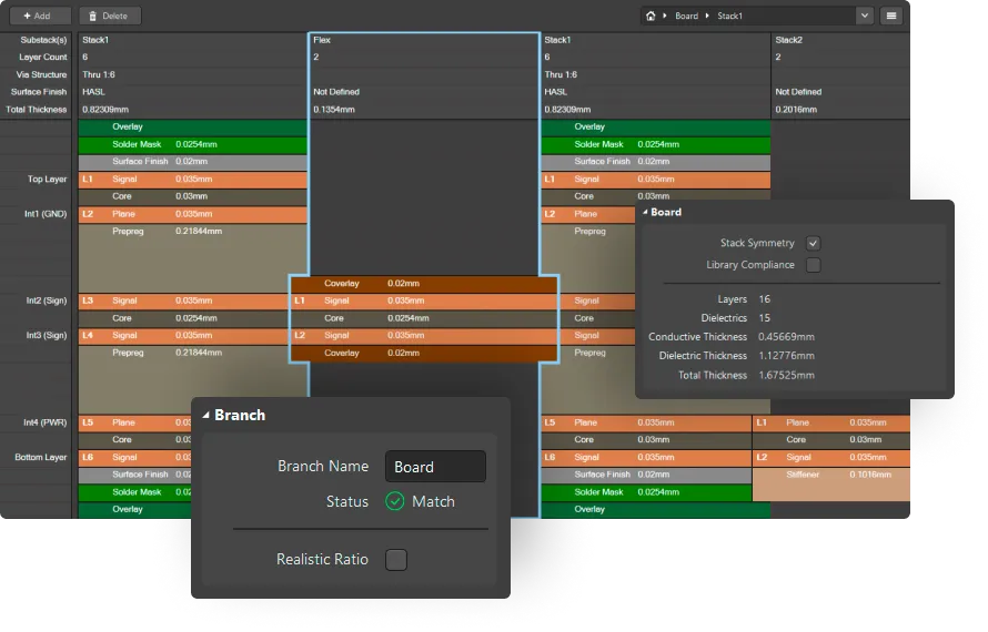
Step 2: Defining Layer Types and Materials
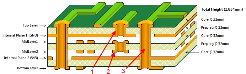
Once your layers are set, assign specific roles to each—signal, ground, or power. Ground and power planes should ideally be placed adjacent to signal layers to provide a return path and reduce noise. In high-speed designs, a common stack-up for a 6-layer board might look like this:
- Layer 1: Signal (Top)
- Layer 2: Ground
- Layer 3: Signal
- Layer 4: Signal
- Layer 5: Power
- Layer 6: Signal (Bottom)
Next, select the dielectric materials between layers. The dielectric constant (Dk) and loss tangent (Df) of the material affect signal speed and loss. For instance, FR-4 has a Dk of about 4.2 at 1 GHz, while high-frequency materials like Rogers 4350B have a Dk of 3.48, offering better performance for signals above 5 GHz.
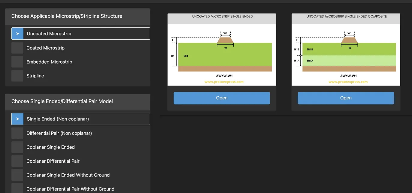
Step 3: Configuring Impedance for Signal Integrity
Impedance control is a cornerstone of signal integrity analysis. High-speed signals, such as those in USB 3.0 (operating at 5 Gbps), require precise impedance matching—often 90 ohms for differential pairs. PCB design software typically includes impedance calculators or simulation tools to help you achieve this.
In the software, input the trace width, spacing, and dielectric thickness to calculate impedance. If the calculated value deviates from your target (e.g., 50 ohms for single-ended traces), adjust the trace width or layer spacing. Many tools also allow you to simulate the signal behavior to check for reflections or crosstalk, ensuring your stack-up supports clean signal transmission.
Running Stack-Up Simulations for Performance
After setting up the stack-up, the next step is to simulate its performance using stack-up simulation features in your PCB design software. Simulation helps identify potential issues like signal delays, crosstalk, or power distribution problems before the board is fabricated.
Step 4: Simulating Signal Integrity
Signal integrity analysis ensures that your signals maintain their quality as they travel across the board. In the simulation module of your software, define the signal nets you want to analyze, such as a high-speed clock signal operating at 200 MHz. The software will model how the signal behaves, considering factors like trace length, layer transitions, and nearby noise sources.
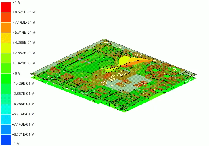
For example, if a simulation shows significant crosstalk (e.g., a voltage spike of 0.5V on an adjacent trace), you can adjust the stack-up by increasing the spacing between signal layers or adding an additional ground plane. Modern tools provide visual graphs of signal waveforms, making it easier to spot issues like overshoot or ringing.
Step 5: Power Distribution Network (PDN) Analysis
A stable power supply is crucial for any PCB, especially in high-speed designs where current demands fluctuate rapidly. PDN analysis within PCB design software evaluates the effectiveness of your power and ground planes in delivering clean power. Look for voltage drops or excessive noise in the simulation results. If the voltage drop exceeds 5% (e.g., dropping from 3.3V to 3.135V), consider widening power traces or adding decoupling capacitors near critical components.
Advanced Tips for Stack-Up Design in High-Speed Applications
For engineers working on complex or high-speed designs, additional considerations can elevate your stack-up design to the next level. Here are some advanced strategies to implement using PCB design software:
Tip 1: Use Blind and Buried Vias
In multi-layer boards, vias connect traces between layers. However, through-hole vias can introduce signal stubs, degrading signal integrity at high frequencies. Blind vias (connecting outer to inner layers) and buried vias (connecting only inner layers) minimize these stubs. Configure these via types in your stack-up editor to optimize routing and reduce signal loss.
Tip 2: Optimize Return Paths
High-speed signals need a continuous return path on an adjacent ground plane to minimize loop inductance. In your stack-up design, ensure that signal layers are always next to a ground plane. If a signal transitions between layers, place vias strategically to maintain the return path, reducing EMI.
Tip 3: Leverage Simulation for Material Selection
Different materials behave differently at various frequencies. Use the simulation tools to test how a material impacts signal loss. For instance, at 10 GHz, a low-loss material might reduce signal attenuation by 20% compared to standard FR-4, justifying the higher cost for critical applications.
Finalizing and Validating Your Stack-Up Design
Once your stack-up is designed and simulated, it’s time to validate the design for manufacturing. Export the stack-up details from your PCB design software, including layer thicknesses, materials, and impedance requirements. Share this documentation with your fabrication team to ensure they can meet the specifications.
Additionally, run a final design rule check (DRC) within the software to catch any errors, such as incorrect layer assignments or impedance mismatches. Address any flagged issues before sending the design for production. A well-validated stack-up design can reduce the risk of costly revisions or performance failures.
Conclusion: Mastering PCB Stack-Up Design with Software
Designing a PCB stack-up is a fundamental skill for any electronics engineer, and using PCB design software makes this process more efficient and accurate. By following the steps outlined in this tutorial—setting up layers, configuring impedance, running simulations, and validating the design—you can create stack-ups that support high-speed signals with excellent signal integrity. Tools like Altium Designer and Cadence Allegro offer powerful features for stack-up simulation and analysis, helping you achieve reliable and high-performing PCB designs.
With practice and the right software, you can tackle even the most complex stack-up challenges, ensuring your designs meet the demands of modern electronics. Keep experimenting with different configurations and simulations to refine your skills and stay ahead in the field of PCB design.


