 ALLPCB


KiCad is a powerful, open-source Electronic Design Automation (EDA) tool that empowers engineers to create professional-grade printed circuit boards (PCBs) without the hefty price tag of commercial software. Whether you're a hobbyist prototyping a new idea or a seasoned engineer designing complex multilayer boards, KiCad's robust features make it an excellent choice for efficient PCB layout design. In this step-by-step guide, we'll walk you through the process of using KiCad to design a PCB layout, offering practical tips and examples to streamline your workflow and ensure high-quality results.
By following this guide, you'll learn how to set up a project, create schematics, assign footprints, lay out your PCB, and generate manufacturing files—all while optimizing for performance and manufacturability. Let's dive in and explore how KiCad can transform your PCB design process.
Why Choose KiCad for PCB Layout Design?
KiCad, a convenient PCB design software, stands out for its versatility and accessibility. It supports up to 32 copper layers, 14 technical layers, and 13 general-purpose drawing layers, making it suitable for everything from simple single-layer boards to complex high-speed designs. Its open-source nature means it's free to use, regularly updated by a dedicated community, and compatible with Windows, macOS, and Linux. Key features like the Interactive Router, 3D Viewer, and Design Rules Checker (DRC) help engineers create precise, error-free layouts efficiently.
For engineers, KiCad's project-based workflow ensures that schematics, layouts, and associated files stay synchronized, reducing errors during design iterations. Whether you're designing a 4 cm circular PCB for a wearable device or a 4 m x 4 m industrial board, KiCad's 1-nanometer internal resolution ensures precision. Let's explore how to leverage these capabilities for an efficient PCB layout.
Step 1: Setting Up Your KiCad Project
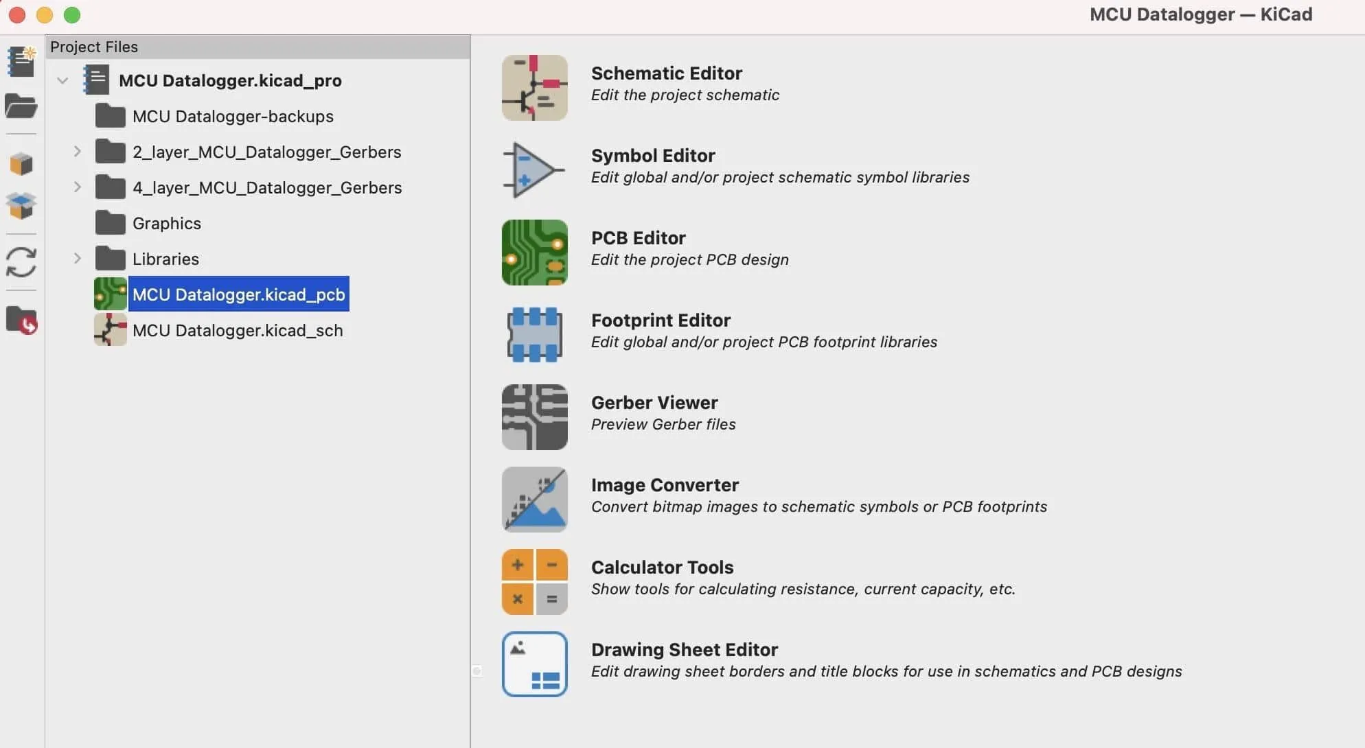
Every KiCad design begins with a new project, which organizes your schematic, PCB layout, and associated files in a single folder. Here's how to get started:
1. Create a New Project
Launch KiCad and navigate to File > New Project. Choose a directory and name your project (e.g., "LED_Board"). KiCad will create a .pro file and a dedicated folder to store all project files.
2. Configure Project Settings
Open the project manager and set the page size to A4 via File > Page Settings. Enter a title (e.g., "LED Board Design") and other details like date and revision to populate the schematic title block.
3. Install Libraries
If prompted, import KiCad'sPaint default symbol and footprint libraries. These include thousands of components, from resistors to microcontrollers, saving you time.
Tip: Always save your project in a synced folder (e.g., Dropbox) to prevent data loss and ensure compatibility across devices.
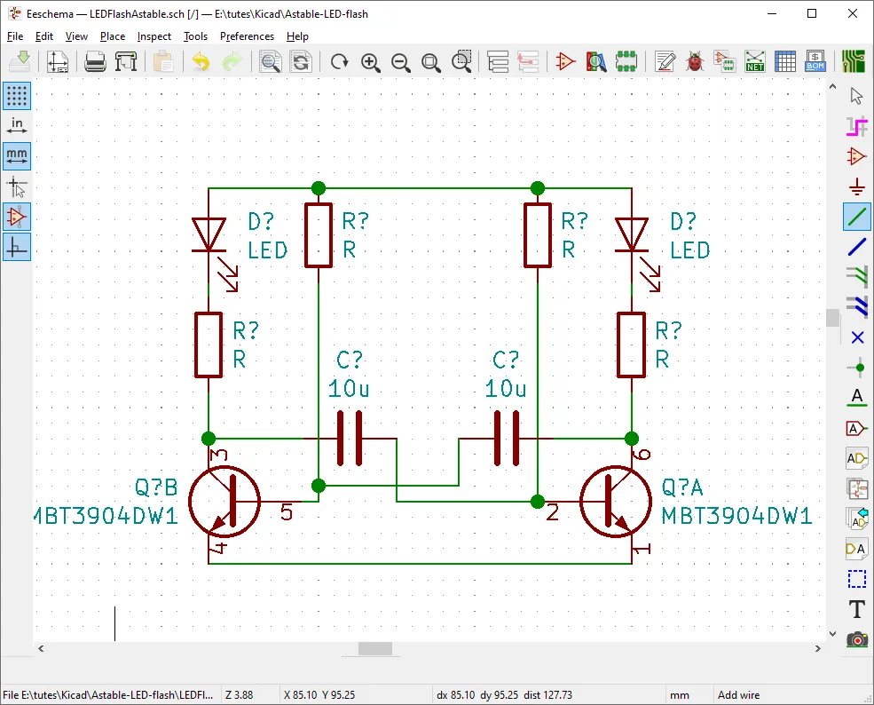
Step 2: Creating the Schematic in Eeschema
The schematic defines your circuit's components and their electrical connections. KiCad's Eeschema editor makes this process intuitive.
1. Open Eeschema
From the project manager, click the Schematic Editor button (first icon on the left).
2. Add Components
Use the Place Symbol tool (or press A) to add components from the library. For example, select a 1 kΩ resistor (R), an LED, and a 5V power symbol. Place them on the canvas.
3. Connect Components
Use the Place Wire tool (W) to draw connections. For instance, connect the resistor in series with the LED's anode, and attach the LED's cathode to ground (GND). Add power flags to 5V and GND to indicate external power sources.
4. Annotate the Schematic
Go to Tools > Annotate Schematic and select Annotate to assign unique reference designators (e.g., R1, D1) to each component. This ensures clarity in the PCB layout.
5. Run Electrical Rules Checker (ERC)
Use Inspect > Electrical Rules Checker to verify connections. Fix errors, such as unconnected pins or missing power flags, to ensure a valid schematic.
Example: For a simple LED circuit, your schematic might include a 1 kΩ resistor (R1) to limit current to 20 mA for a 5V supply, calculated using Ohm's Law: V = IR, where V = 5V - 2V (LED forward voltage) = 3V, and I = 20 mA. Thus, R = 3V / 0.02A = 150Ω, but a 1 kΩ resistor is used for safety and lower brightness.
Step 3: Assigning Footprints
Footprints define how components are physically placed and soldered on the PCB. Assigning correct footprints is critical for a manufacturable design.
1. Open Footprint Assignment Tool
In Eeschema, go to Tools > Assign Footprints to open the Footprint Assignment window.
2. Select Footprints
For each component, choose an appropriate footprint. For example, select a through-hole (THT) resistor footprint (e.g., Resistor_THT:R_Axial_DIN0207) for R1 and an LED footprint (e.g., LED_THT:LED_D5.0mm) for the LED. For surface-mount designs, choose SMD footprints like Resistor_SMD:R_0805.
3. Verify Assignments
Double-check that footprints match your components' physical dimensions and pin configurations to avoid manufacturing issues.
Tip: Use KiCad's footprint library filters to narrow down options by package type (e.g., THT vs. SMD) or size.
Step 4: Laying Out the PCB in Pcbnew
With the schematic complete, it's time to design the physical PCB layout in KiCad's Pcbnew editor.
1. Import the Netlist
Open Pcbnew from the project manager and go to Tools > Update PCB from Schematic (or press F8). This imports components and connections from the schematic, placing them on the canvas with white "rat's nest" lines indicating connections.
2. Define the Board Outline
Use the Edge.Cuts layer to draw the board shape. For example, create a 3 cm x 3 cm rectangular board using the Draw Rectangle tool. Ensure the outline is a closed shape for 3D rendering and manufacturing.
3. Place Components
Arrange components strategically. Place critical components like connectors or microcontrollers first, followed by supporting components like resistors. For high-speed signals (e.g., 100 MHz), keep trace lengths short to minimize impedance (typically 50 Ω for controlled impedance lines).
4. Route Traces
Use the Route Tracks tool (X) to draw copper traces. KiCad's Interactive Router offers three modes:
- Highlight Collision: Shows trace interference.
- Shove: Pushes existing traces to make room.
- Walkaround: Routes around obstacles.
For a 20 mA LED circuit, use a 0.25 mm trace width, sufficient for low-current signals.
5. Add Vias and Layers
For multilayer boards, use vias to connect traces between layers. For example, route a ground plane on the bottom layer and signal traces on the top layer, using 0.8 mm vias.
Step 5: Setting Design Rules
Design rules ensure your PCB meets manufacturing requirements and performs reliably.
1. Access Design Rules
In Pcbnew, go to File > Board Setup > Design Rules. Set clearances and track widths based on your manufacturer's specifications (e.g., 0.25 mm clearance, 0.25 mm minimum track width for standard 1.6 mm boards).
2. Create Net Classes
Group nets (e.g., power, signal) and assign rules. For example, set power nets to 1 mm track width for 1 A current and signal nets to 0.25 mm for 100 mA.
3. Add Custom Rules
Use the Custom Rules section to define specific constraints, such as a 0.5 mm clearance between vias on different nets to prevent shorts.
Tip: Check your manufacturer's design rule guidelines. For instance, a typical 2-layer board requires a minimum drill size of 0.3 mm and an annular ring of 0.15 mm.
Step 6: Running Design Rules Checker (DRC)
The DRC verifies that your layout complies with design rules and schematic connections.
1. Run DRC
Go to Inspect > Design Rules Checker and click Run DRC. Enable Refill all zones for accurate results.
2. Review Errors
Check the DRC window for violations, such as "Via near track" or "Pad near pad." For example, a "Via near track" error indicates a via is closer than the 0.25 mm clearance rule.
3. Fix Issues
Adjust traces or components to resolve errors. For instance, reroute a trace using the Delete (Del) and Route Tracks (X) tools to increase clearance.
Step 7: Generating Manufacturing Files
Once your layout passes DRC, generate files for manufacturing.
1. Generate Gerber Files
In Pcbnew, go to File > Fabrication Outputs > Gerbers. Select all necessary layers (e.g., F.Cu, B.Cu, F.Silkscreen, Edge.Cuts) and output to a folder.
2. Create Drill Files
In the same menu, select Generate Drill Files. Merge PTH and NPTH holes into one file for simplicity.
3. Export Bill of Materials (BOM)
In Eeschema, go to Tools > Generate Bill of Materials to create a component list for assembly.
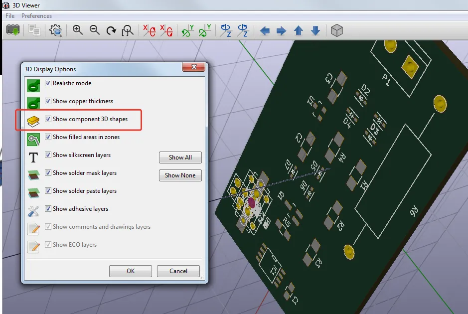
4. Preview in 3D Viewer
Use View > 3D Viewer to inspect the board for mechanical fit and aesthetics. Switch to raytracing mode for a realistic render.
Tip: Verify Gerber files using a viewer like GerbView to ensure all layers are correct before submission.
Leveraging ALLPCB for Seamless PCB Manufacturing
Once your KiCad design is complete, partnering with a reliable manufacturer is key to bringing your PCB to life. ALLPCB offers quick-turn prototyping, with lead times as short as 24 hours for 2-layer boards, ensuring you can iterate rapidly. Our global logistics network delivers boards worldwide, and our advanced manufacturing capabilities support complex designs with up to 6 layers and precise solder mask alignment. By uploading your KiCad-generated Gerber files to ALLPCB's online platform, you can get an instant quote, select options like 1.6 mm thickness or blue solder mask, and track your order in real-time, making the transition from design to production seamless.
Tips for Efficient PCB Layout in KiCad
Optimize component placement: Place components to minimize trace lengths, especially for high-speed signals (e.g., keep USB traces under 100 mm to reduce signal degradation).
Use the Interactive Router: Switch to Shove mode for complex layouts to automatically adjust existing traces.
Run DRC frequently: Check for errors after major changes to catch issues early.
Document your design: Add text to the silkscreen layer for component designators and notes to aid assembly.
Conclusion
KiCad is a game-changer for PCB layout design, offering engineers a free, powerful tool to create professional-grade boards with precision and efficiency. By following this step-by-step guide—setting up a project, creating schematics, assigning footprints, laying out the board, setting design rules, running DRC, and generating manufacturing files—you can streamline your design process and achieve high-quality results. Whether you're designing a simple LED circuit or a multilayer high-speed board, KiCad's features like the Interactive Router and 3D Viewer empower you to tackle any project with confidence.
Ready to turn your KiCad design into reality? Upload your Gerber files to ALLPCB for fast, reliable manufacturing and bring your ideas to life. Start designing today and unlock the full potential of your PCB projects!


