ALLPCB


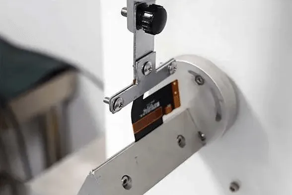
Wearable devices, from fitness trackers to smartwatches, demand compact, lightweight, and durable electronics that can conform to the human body. Flexible printed circuit boards (PCBs) are the backbone of these devices, enabling designs that bend and flex without compromising performance. However, improper bend radius planning can lead to mechanical failure, signal degradation, or reduced product lifespan. In this guide, we explore the critical aspects of flex PCB ? radius planning for wearable devices, offering engineers actionable insights to optimize their designs for reliability and manufacturability.
Understanding bend radius—the minimum radius a flex PCB can bend without damage—is essential for ensuring durability in dynamic applications like wearables. By carefully calculating bend radius, selecting appropriate materials, and adhering to best practices, engineers can create robust designs that meet the stringent demands of modern wearable technology.
What Is Flex PCB Bend Radius?
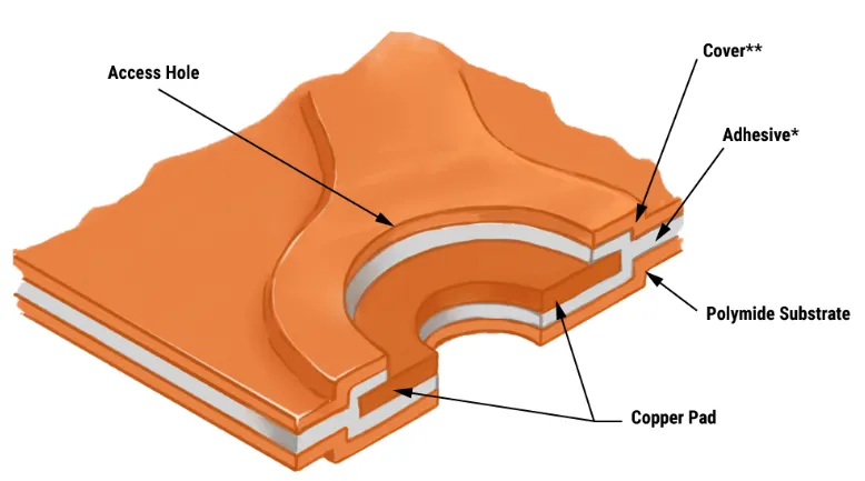
The bend radius of a flex PCB is defined as the minimum radius at which the board can be bent without causing damage to the copper traces, dielectric substrate, or overall circuit integrity. In wearable devices, where PCBs must conform to curved surfaces or endure repeated flexing, the bend radius directly impacts reliability and longevity. A smaller bend radius increases flexibility but heightens the risk of mechanical stress, copper cracking, or delamination.
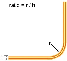
For wearable applications, the bend radius depends on factors like the number of layers, material thickness, and whether the PCB is designed for static (bent once during installation) or dynamic (repeated flexing) use. According to IPC-2223 standards, the minimum bend radius for a single-layer flex PCB in static applications is typically 6 times the board thickness, while dynamic applications require a minimum of 100 times the thickness to ensure long-term reliability.
Why Bend Radius Matters in Wearable Devices
Wearable devices, such as smartwatches or medical sensors, often operate in dynamic environments where the PCB must flex repeatedly without failing. A poorly planned bend radius can lead to:
-
Copper Trace Fractures: Excessive bending causes stress concentration, leading to cracks in copper traces, which disrupt electrical connectivity.
-
Dielectric Damage: Overstretching the substrate (e.g., polyimide) can cause delamination or tearing, compromising insulation.
-
Signal Integrity Issues: Tight bends may alter impedance, especially in high-speed designs, leading to signal degradation.
-
Reduced Lifespan: In dynamic applications, improper bend radii accelerate fatigue, shortening the device's operational life.
For example, a fitness tracker wrapped around a wrist may require a bend radius as tight as 10 mm to fit the device's compact enclosure. If the PCB's minimum bend radius is not calculated correctly, repeated flexing could cause trace failure within weeks, leading to costly returns or redesigns.
Key Factors Influencing Bend Radius
To plan an effective bend radius for wearable devices, engineers must consider several interdependent factors:
1. Number of Layers
The number of conductive layers in a flex PCB significantly affects its flexibility. Single- and double-layer flex PCBs are ideal for dynamic applications due to their thinner profiles and lower stiffness. For instance, a single-layer flex PCB with a thickness of 0.1 mm can achieve a minimum bend radius of 1 mm in static applications. In contrast, multilayer PCBs (three or more layers) require larger bend radii—typically 20-25 times the total thickness—due to increased rigidity and stress concentration.
2. Material Selection
The choice of substrate and copper thickness plays a critical role. Polyimide (PI) is the most common substrate for flex PCBs in wearables due to its high flexibility, thermal stability, and durability. Thinner polyimide films (e.g., 12.5 μm vs. 25 μm) allow for smaller bend radii but may require careful handling during manufacturing. Similarly, reducing copper thickness from 35 μm to 17.5 μm can increase flexibility and boost flex cycle life from 20,000 to 90,000 cycles in dynamic applications.
3. Static vs. Dynamic Applications
Static flex PCBs, bent once during assembly (e.g., in a folded smartwatch strap), can tolerate tighter bend radii. Dynamic flex PCBs, which endure repeated bending (e.g., in a medical wearable that flexes with body movement), require larger radii to prevent fatigue. For dynamic applications, a bend radius of 100 times the board thickness is a common guideline to ensure reliability over millions of flex cycles.
4. Trace and Via Placement
Routing traces perpendicular to the bend axis minimizes stress and prevents copper breakage. Avoid placing vias or plated through-holes within 20 mil of the bend area, as they can create weak points prone to cracking. Staggering traces on multilayer designs also reduces the "I-beam effect," where stacked traces increase stiffness and stress.
5. Environmental Conditions
Wearables are exposed to temperature fluctuations, humidity, and mechanical vibrations. These factors can exacerbate stress in tight bends, especially in high-temperature environments where thermal expansion increases mechanical strain. Selecting materials with low thermal expansion coefficients (e.g., polyimide over polyester) ensures reliability under varying conditions.
Calculating the Bend Radius
To calculate the minimum bend radius, engineers can use guidelines from IPC-2223 or manufacturer-specific recommendations. The formula varies based on the application and layer count:
-
Single-Layer, Static: Minimum bend radius = 6 × total thickness
-
Single-Layer, Dynamic: Minimum bend radius = 100 × total thickness
-
Multilayer, Static: Minimum bend radius = 10-20 × total thickness
-
Multilayer, Dynamic: Minimum bend radius = 100-150 × total thickness
For example, a double-layer flex PCB with a total thickness of 0.2 mm (including 25 μm polyimide, 17.5 μm copper, and 25 μm coverlay) would have a minimum bend radius of 2 mm for static applications (10 × 0.2 mm) and 20 mm for dynamic applications (100 × 0.2 mm). Engineers should verify these calculations using finite element analysis (FEA) tools to simulate bending stress and identify potential failure points.
Best Practices for Bend Radius Planning
To optimize flex PCB designs for wearable devices, follow these best practices:
1. Minimize Layer Count
Where possible, limit the design to one or two layers to maximize flexibility and reduce costs. For high-density designs requiring more layers, use the bookbinding technique, where flex layers are progressively lengthened to reduce stress during tight bends. This method is costly but effective for multilayer designs with bend radii below 6 times the thickness.
2. Use Adhesive-Less Materials
Adhesive-based laminates can cause issues like via cracks or dimensional errors during bending. Adhesive-less polyimide laminates are thinner, more flexible, and resistant to moisture absorption, making them ideal for wearables. They also improve impedance control, critical for high-speed signals in devices like 5G-enabled smartwatches.
3. Incorporate Stiffeners and Cutouts
For designs with surface-mount components, add stiffeners (e.g., FR4 or polyimide) to reinforce areas outside the bend zone. In regions without traces, insert circular cutouts with radii greater than 30 mil to reduce material deformation and enhance flexibility.
4. Optimize Trace Layout
Use curved traces instead of sharp angles to minimize stress concentration. Taper pads where traces enter to prevent weak spots, and maintain a minimum 10 mil clearance between adjacent flex regions to avoid mechanical interference.
5. Conduct Rigorous Testing
Simulate bending and flexing using advanced design tools during the design phase. After prototyping, perform flex endurance testing (e.g., 100,000 cycles at the target bend radius) and thermal cycling to validate performance under real-world conditions. This is critical for wearables, where reliability is non-negotiable.
Common Mistakes to Avoid
Even experienced engineers can make errors in bend radius planning. Here are pitfalls to watch for:
-
Ignoring Layer Stackup: Failing to account for the cumulative thickness of all layers can lead to an underestimated bend radius, causing premature failure.
-
Overlapping Traces: Stacking traces directly over each other in multilayer designs increases stiffness and stress, reducing flexibility.
-
Placing Components in Bend Areas: Components in the bend zone, especially in dynamic applications, can crack or detach. For static bends, small, non-fragile components may be placed in concave areas with a minimum bend radius of 100 mm.
-
Neglecting Environmental Factors: Wearables often face moisture, heat, or vibration. Choosing materials without adequate environmental resilience can degrade performance over time.
How ALLPCB Supports Flex PCB Design
For engineers designing flex PCBs for wearable devices, partnering with a reliable manufacturer is critical to success. ALLPCB's advanced manufacturing capabilities, quick-turn prototyping, and global logistics ensure that your designs are brought to life with precision and efficiency. Our state-of-the-art facilities support adhesive-less polyimide laminates, precise layer stackups, and rigorous quality testing to meet the demands of dynamic applications. Whether you need prototypes to validate bend radius calculations or high-volume production for a new wearable device, the expertise and commitment to quality from ALLPCB help you achieve reliable, high-performance flex PCBs.
Conclusion
Flex PCB bend radius planning is a critical step in designing reliable and durable wearable devices. By understanding the factors that influence bend radius—such as layer count, material selection, and application type—engineers can create designs that balance flexibility with performance. Following best practices, like minimizing layers, using adhesive-less materials, and conducting thorough testing, ensures that flex PCBs withstand the mechanical and environmental stresses of wearable applications.
As wearable technology continues to evolve, precise bend radius planning will remain a cornerstone of innovative design. By leveraging simulation tools, adhering to industry standards, and collaborating with experienced manufacturers, engineers can push the boundaries of what's possible in compact, dynamic electronics.