 ALLPCB


For electrical engineers working on printed circuit board (PCB) assembly, ensuring quality and reliability is paramount. One of the most powerful tools to achieve this is X-Ray inspection. But what exactly is PCB X-Ray inspection, and how does it help in detecting hidden defects like solder joint voids or issues in Ball Grid Array (BGA) components? In short, PCB X-Ray inspection is a non-destructive testing method that uses X-rays to reveal internal structures and defects in assembled PCBs, such as voids in solder joints, misalignments in BGAs, and flaws in multilayer boards. This blog post takes a deep dive into the PCB X-Ray inspection process, exploring solder joint void detection, BGA X-Ray analysis, multilayer PCB defect analysis, and the importance of X-Ray machine resolution. Whether you're troubleshooting a failed prototype or ensuring production quality, this guide will provide actionable insights to help you master this critical technology.
Why PCB X-Ray Inspection Matters for Engineers
As an electrical engineer, you know that modern PCBs are becoming increasingly complex with smaller components, denser layouts, and multilayer designs. Surface-level inspections like Automated Optical Inspection (AOI) can catch visible flaws, but what about defects hidden beneath components or within layers? This is where PCB X-Ray inspection shines. It allows you to see inside the board without damaging it, making it a vital part of quality control in electronics manufacturing. From detecting solder joint voids that could lead to electrical failures to analyzing BGAs for connection issues, X-Ray inspection ensures your designs meet reliability standards.
Understanding the PCB X-Ray Inspection Process
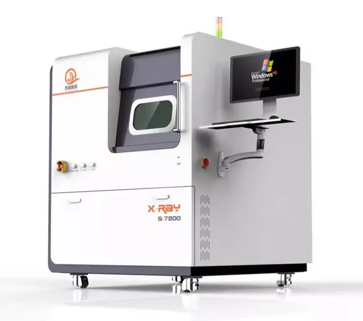
The PCB X-Ray inspection process is a systematic approach to uncovering internal defects in assembled boards. It uses Automated X-Ray Inspection (AXI) systems, which emit X-rays to penetrate the PCB and create detailed images of its internal structure. Here's a breakdown of the key steps:
- Setup and Calibration: The PCB is placed in the X-Ray machine, and the system is calibrated based on the board's material and thickness. For instance, a typical multilayer PCB might require an X-Ray voltage of 80-120 kV to penetrate copper layers effectively.
- Image Capture: X-rays pass through the PCB, and a detector captures the transmitted rays to form a 2D or 3D image. Dense materials like solder appear darker, while less dense areas like voids appear lighter.
- Analysis: Engineers or automated software analyze the images for defects. This could include checking for solder joint voids, misaligned BGA balls, or cracks in vias.
- Reporting: Findings are documented, often with annotated images, to guide rework or process improvements.
For engineers, understanding this process is crucial when selecting an X-Ray system or interpreting results. Knowing the machine's capabilities, such as its resolution and penetration depth, can help you ensure accurate defect detection in your specific PCB designs.
Solder Joint Void Detection: Ensuring Reliable Connections
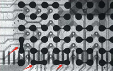
Solder joint voids are air pockets or gaps within the solder that connects components to the PCB. These voids can weaken the mechanical and electrical connection, leading to failures over time, especially in high-stress environments. X-Ray inspection is the go-to method for solder joint void detection because it can reveal these hidden flaws without disassembling the board.
During X-Ray analysis, voids appear as lighter spots within the darker solder joint area due to their lower density. Industry standards, such as IPC-A-610, often specify acceptable void percentages—typically less than 25% of the joint area for most applications. For a BGA component with hundreds of solder joints, manually inspecting each one would be impossible without X-Ray technology. Advanced systems can even quantify void size and location, helping engineers pinpoint problematic areas. For example, a void larger than 30% in a critical power connection might require rework to prevent overheating or signal loss.
As an engineer, you can use these insights to adjust soldering parameters, such as reflow temperature profiles (e.g., peak temperatures of 235-245°C for lead-free solder), to minimize void formation during assembly.
BGA X-Ray Analysis: Peeking Under the Package
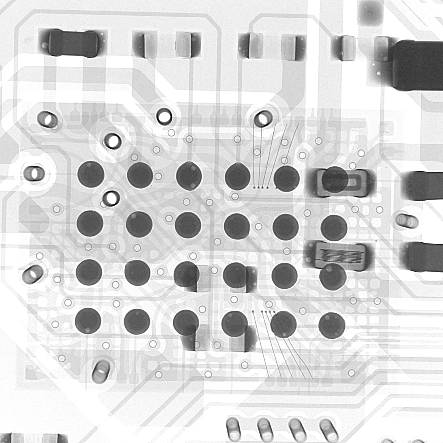
Ball Grid Array (BGA) components are widely used in modern electronics due to their high pin density and compact size. However, their solder connections are hidden beneath the package, making traditional visual inspection impossible. BGA X-Ray analysis solves this by providing a clear view of the solder balls and their connections to the PCB pads.
Common defects in BGAs include bridging (solder connecting adjacent balls), insufficient solder, and misalignment. X-Ray images can reveal if a solder ball has collapsed—indicating poor reflow—or if there's a "head-in-pillow" defect, where the ball appears connected but lacks a proper metallurgical bond. For instance, a typical BGA might have solder balls with a diameter of 0.3-0.5 mm, and an X-Ray system with a resolution of 5 micrometers can easily detect deviations as small as 10% in ball size or spacing.
For engineers, BGA X-Ray analysis is critical when debugging prototypes or validating high-volume production. It helps ensure signal integrity, especially in high-speed designs where a single poor connection can cause data errors at frequencies above 1 GHz.
Multilayer PCB Defect Analysis: Seeing Through the Layers
Multilayer PCBs, often with 4 to 16 layers or more, are the backbone of complex electronics like smartphones and medical devices. Defects in internal layers—such as delamination, via cracks, or misregistration—can be catastrophic yet invisible to the naked eye. Multilayer PCB defect analysis using X-Ray inspection allows engineers to examine these hidden structures non-destructively.
X-Ray systems equipped with 3D computed tomography (CT) or laminography can reconstruct detailed cross-sectional views of a multilayer PCB. For example, a via with a diameter of 0.2 mm might show a hairline crack under X-Ray, indicating a potential open circuit. Similarly, misalignment between layers, even by as little as 0.1 mm, can be detected and correlated with signal integrity issues in high-frequency applications (e.g., impedance mismatches at 50 ohms).
For electrical engineers, this level of analysis is invaluable when designing or troubleshooting multilayer boards. It helps identify manufacturing issues early, reducing costly redesigns or field failures. Recent advancements, such as those discussed in industry articles, highlight how 3D X-Ray techniques improve defect detection in complex multilayer designs, ensuring reliability in demanding applications.
The Role of X-Ray Machine Resolution in Defect Detection
Not all X-Ray machines are created equal, and resolution is a critical factor for effective PCB inspection. X-Ray machine resolution determines the smallest defect or feature the system can detect, typically measured in micrometers (μm). For instance, a high-resolution system with a capability of 1-5 μm can identify tiny voids or cracks in solder joints, while a lower-resolution system (10-20 μm) might miss these subtle flaws.
Resolution also affects the clarity of images for small components. In a QFN (Quad Flat No-Lead) package with lead pitches of 0.4 mm, a high-resolution X-Ray system ensures that each connection is clearly visible, allowing for precise defect analysis. However, higher resolution often comes with trade-offs, such as longer inspection times or higher equipment costs. For production environments, engineers must balance resolution needs with throughput— a system with 5 μm resolution might take 30 seconds per board, while a 10 μm system could inspect in half that time.
When selecting or using an X-Ray system, consider the specific requirements of your PCB design. For high-density boards with fine-pitch components, prioritize resolution over speed. For larger, less complex boards, a mid-range resolution might suffice. Understanding these trade-offs can help you optimize inspection without compromising quality.
Benefits of PCB X-Ray Inspection for Quality Assurance
Integrating X-Ray inspection into your PCB assembly workflow offers several benefits, especially for engineers focused on quality and reliability:
- Non-Destructive Testing: Unlike cross-sectioning or other destructive methods, X-Ray inspection preserves the PCB for further use or rework.
- Comprehensive Defect Detection: It uncovers hidden issues in solder joints, BGAs, and multilayer structures that other methods like AOI cannot detect.
- Process Improvement: By identifying root causes of defects (e.g., insufficient solder paste volume or incorrect reflow profiles), X-Ray analysis helps refine manufacturing processes.
- Cost Savings: Early defect detection reduces scrap rates and prevents expensive field failures. For example, catching a BGA misalignment in prototype testing can save thousands in warranty claims.
For engineers, these advantages translate to higher confidence in your designs and faster time-to-market, especially in industries like automotive or aerospace where reliability is non-negotiable.
Challenges and Best Practices in PCB X-Ray Inspection
While X-Ray inspection is powerful, it’s not without challenges. High-density boards can produce cluttered images, making defect identification tricky. Additionally, X-Ray systems require skilled operators or advanced software to interpret results accurately. Radiation safety is another concern, though modern systems are designed with shielding to minimize risks.
Here are some best practices for engineers:
- Use Automated Analysis: Invest in software that automatically detects and classifies defects to reduce human error.
- Regular Calibration: Ensure the X-Ray machine is calibrated frequently to maintain image accuracy, especially for high-resolution scans.
- Focus on Critical Areas: Prioritize inspecting high-risk components like BGAs or power connections to optimize inspection time.
- Collaborate with Manufacturers: Work with your PCB assembly partner to correlate X-Ray findings with process data, such as stencil design or reflow settings.
By following these practices, you can maximize the effectiveness of X-Ray inspection in your workflow.
Conclusion: Harnessing X-Ray Inspection for PCB Excellence
PCB X-Ray inspection is an indispensable tool for electrical engineers striving to build reliable, high-quality electronics. From the detailed PCB X-Ray inspection process to specialized applications like solder joint void detection, BGA X-Ray analysis, and multilayer PCB defect analysis, this technology uncovers hidden flaws that could otherwise lead to failure. Understanding factors like X-Ray machine resolution ensures you choose the right system for your needs, balancing precision with efficiency.


