 ALLPCB


If you're looking to create an SMD PCB stencil and frame for precise solder paste application, you've come to the right place. At ALLPCB, we understand the importance of accuracy in surface mount device (SMD) assembly. In this guide, we'll walk you through the process of building an effective stencil and frame using tools like CadSoft Eagle and materials such as Kapton film. Whether you're a hobbyist or a professional, this step-by-step tutorial will help you achieve professional results for your SMD PCB projects.
Below, we dive into the detailed process, from design to assembly, ensuring you have all the tools and knowledge needed to succeed. Let's get started with everything you need to know about crafting an SMD PCB stencil and frame.
Why You Need an SMD PCB Stencil and Frame
When working on SMD PCB projects, applying solder paste accurately is critical for ensuring proper component placement and reliable connections. An SMD PCB stencil acts as a template, allowing you to deposit solder paste only where it's needed. Pairing it with a sturdy frame makes the process even more efficient, especially for small boards or batch production. A frame holds the stencil taut and in place, preventing misalignment during application.
Using tools like CadSoft Eagle for design and materials like Kapton film for durability, you can create custom stencils tailored to your board's layout. This approach saves time, reduces errors, and improves the quality of your soldering, particularly for intricate designs with fine-pitch components.
Materials and Tools for Building Your Stencil and Frame
Before diving into the construction process, gather the necessary materials and tools. Here's a comprehensive list to ensure you're fully prepared:
- Kapton Film: A heat-resistant, flexible polyimide film ideal for laser-cut stencils. It can withstand high temperatures during soldering without deforming.
- Stencil Frame Material: Aluminum or wooden frames work well for holding the stencil in place. Choose a size slightly larger than your PCB design.
- CadSoft Eagle Software: A powerful tool for designing PCB layouts and generating stencil files.
- Laser Cutter or CNC Machine: Essential for cutting precise openings in the Kapton film based on your design.
- Adhesive or Tape: To secure the Kapton film to the frame without wrinkles or gaps.
- Solder Paste: For testing the stencil after assembly.
- PCB Board: A sample board to align and test your stencil.
- Basic Tools: Scissors, ruler, and a cutting mat for manual adjustments if needed.
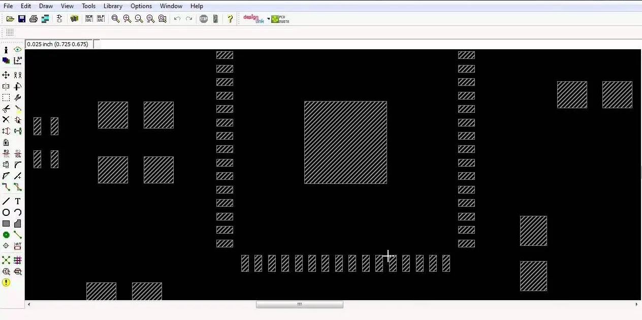
Step 1: Designing Your Stencil Using CadSoft Eagle
The first step in building your SMD PCB stencil is creating a precise design that matches your PCB layout. CadSoft Eagle is an excellent choice for this task due to its user-friendly interface and robust features for PCB design.
- Open Your PCB Layout: Load your existing PCB project in CadSoft Eagle. Ensure all SMD components are correctly placed in the layout editor.
- Access the Cream Layer: In Eagle, the solder paste layer is often called the "Cream" or "tCream" layer. This layer defines where solder paste will be applied. Make sure only the pads for SMD components are visible on this layer.
- Adjust Pad Openings: For fine-pitch components, reduce the cream layer openings by about 10-20% compared to the actual pad size to prevent excess solder paste. For example, if a pad is 1.0mm wide, set the cream layer opening to 0.8-0.9mm.
- Export the Stencil File: Once your cream layer is finalized, export it as a Gerber file. This file will be used to cut the stencil pattern into the Kapton film. Use the CAM processor in Eagle to generate the Gerber file for the top cream layer (and bottom if applicable).
Step 2: Preparing the Kapton Film for Stencil Cutting
Kapton film is a popular choice for DIY stencils because of its durability and heat resistance. It can handle temperatures up to 400°C, making it perfect for reflow soldering processes. Here's how to prepare it:
- Select the Right Thickness: Choose a Kapton film thickness between 0.05mm and 0.1mm. Thinner films are better for fine-pitch components, while thicker films offer more durability for repeated use.
- Cut to Size: Measure your frame dimensions and cut the Kapton film to fit, leaving an extra 2-3cm on each side for secure attachment.
- Load into Cutting Machine: Place the Kapton film into your laser cutter or CNC machine. Ensure it lies flat to avoid uneven cuts. If using a laser cutter, set the power to a low setting (around 10-15W) to prevent burning the film.
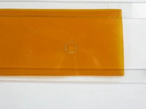
Step 3: Cutting the Stencil Pattern
With your Gerber file ready and the Kapton film loaded, it's time to cut the stencil pattern. Precision is key here to ensure the solder paste is applied accurately.
- Import the Gerber File: Load the cream layer Gerber file into your cutting machine's software. Double-check the scale to match your PCB dimensions.
- Set Cutting Parameters: For laser cutting Kapton film, use a speed of 50-100mm/s and adjust the power based on trial cuts. Start with lower settings to avoid melting the material.
- Cut the Stencil: Execute the cutting process. Once done, carefully remove the Kapton film and inspect the openings. Use a magnifying glass to check for burrs or incomplete cuts, and clean them up with a fine blade if necessary.
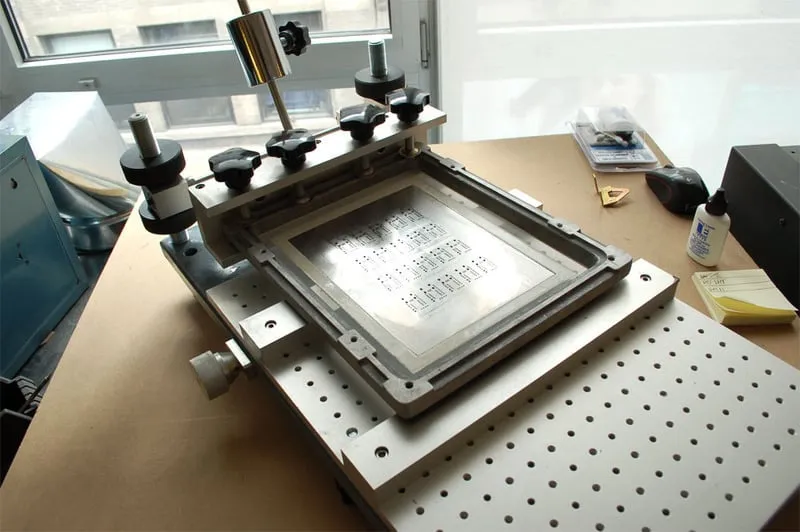
Step 4: Building and Attaching the Frame
A frame is essential for keeping the stencil flat and aligned during solder paste application. Here's how to build and attach it:
- Choose or Build a Frame: Use a pre-made aluminum frame or construct a simple wooden frame. Ensure the inner dimensions are at least 5cm larger than your PCB on all sides for easy handling.
- Attach the Kapton Stencil: Lay the cut Kapton film over the frame. Pull it taut to avoid wrinkles, and secure it with high-temperature adhesive or heat-resistant tape. Start from one side and work your way around to maintain even tension.
- Trim Excess Material: Once secured, trim any overhanging Kapton film for a neat appearance.
Step 5: Testing Your Stencil and Frame
Before using your stencil for a full production run, test it to ensure accuracy and alignment.
- Align with a Sample PCB: Place your PCB under the stencil and align the openings with the pads. Use tape to secure the PCB in place if needed.
- Apply Solder Paste: Use a squeegee to spread solder paste over the stencil. Apply even pressure at a 45-degree angle to push the paste through the openings. A typical solder paste thickness after application should be around 0.1-0.15mm for most SMD components.
- Inspect the Results: Lift the stencil carefully and check the solder paste deposits on the PCB. Look for uniform coverage and clean edges. If you notice bridging or insufficient paste, adjust the stencil design or application technique.
Tips for Success with SMD PCB Stencils
To ensure the best results with your stencil and frame, keep these practical tips in mind:
- Clean Regularly: After each use, clean the stencil with isopropyl alcohol and a soft cloth to remove residual solder paste. This prevents clogging and extends the stencil's life.
- Store Properly: Store the stencil flat in a dry, dust-free environment to avoid damage to the Kapton film.
- Check Alignment Frequently: Misalignment can lead to soldering defects. Always double-check the stencil's position before applying solder paste.
- Experiment with Solder Paste Volume: Different components may require varying amounts of solder paste. For instance, larger components like capacitors may need a slightly thicker deposit (up to 0.2mm) compared to fine-pitch ICs.
Advantages of Using Kapton Film for Stencils
Kapton film offers several benefits that make it an excellent material for SMD PCB stencils:
- Heat Resistance: With a melting point above 400°C, Kapton withstands reflow soldering temperatures without warping.
- Flexibility: Its thin, flexible nature allows for precise cutting and easy handling, even for intricate designs.
- Cost-Effective: Compared to stainless steel stencils, Kapton film is more affordable for small-scale or prototype projects.
Common Challenges and How to Overcome Them
Building and using an SMD PCB stencil can come with a few hurdles. Here's how to address them:
- Uneven Cuts in Kapton Film: If your laser cutter leaves rough edges, reduce the power or speed settings. Test on a scrap piece first to find the optimal parameters.
- Stencil Misalignment: Use registration marks on both the PCB and stencil during design in CadSoft Eagle. These marks help align the stencil accurately each time.
- Solder Paste Smearing: Apply paste with a consistent angle and pressure. If smearing occurs, ensure the stencil is clean and the PCB is firmly secured.
Conclusion: Elevate Your SMD PCB Assembly with Custom Stencils
Building an SMD PCB stencil and frame is a game-changer for anyone involved in electronics assembly. By using tools like CadSoft Eagle to design your stencil and durable materials like Kapton film for construction, you can achieve precision and efficiency in your projects. A well-made stencil and frame setup not only saves time but also enhances the quality of your soldering, ensuring reliable connections for even the smallest SMD components.
At ALLPCB, we're committed to supporting your PCB assembly needs with resources and expertise. Follow the steps outlined in this guide to create your own stencil and frame, and take your SMD PCB projects to the next level. With practice, you'll master the art of solder paste application and produce professional-grade boards with ease.


