 ALLPCB


If you're looking to master SMD PCB design, you're in the right place. This tutorial will guide you through the essentials of designing surface-mount device (SMD) printed circuit boards (PCBs), from creating footprints to component placement and reflow soldering techniques. Whether you're a beginner or an experienced engineer, this guide offers actionable steps to improve your skills and achieve reliable, high-quality results. Let's dive into the detailed process of SMD PCB design, covering everything you need to know to succeed.
What is SMD PCB Design and Why Does It Matter?
SMD PCB design focuses on creating boards that use surface-mount technology (SMT), where components are mounted directly onto the surface of the PCB rather than through holes. This method allows for smaller, lighter, and more compact designs, making it ideal for modern electronics like smartphones, wearables, and IoT devices. Mastering SMD PCB design is crucial because it ensures better performance, reduces manufacturing costs, and meets the demands of high-density layouts.
In this comprehensive tutorial, we'll break down the key aspects of SMD PCB design, including footprint creation, component placement guidelines, and reflow soldering techniques. By the end, you'll have a solid foundation to create efficient and reliable SMD-based PCBs.
Step 1: Understanding SMD Footprint Creation
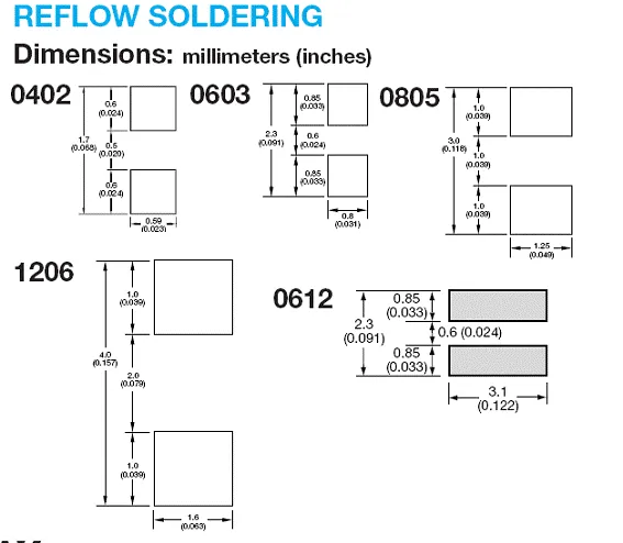
Creating accurate SMD footprints is the foundation of any successful PCB design. A footprint is the physical layout on the PCB where an SMD component will be soldered. If the footprint is incorrect, the component won't fit or connect properly, leading to assembly issues or circuit failure.
To create an SMD footprint, start by referring to the component's datasheet. Manufacturers provide detailed dimensions for the component's body, leads, and recommended pad sizes. For example, a typical 0805 resistor (0.08 inches by 0.05 inches) might have a recommended pad size of 1.0 mm by 0.6 mm with a gap of 1.2 mm between pads. Use design software to draw the pads, ensuring they match the specified dimensions. Add a silkscreen outline to indicate the component's position and orientation for easier assembly.
Pay attention to tolerances as well. Pads that are too small can cause soldering issues, while pads that are too large might lead to tombstoning, where one end of the component lifts during soldering. A good rule of thumb is to extend the pad length by about 0.2 mm beyond the component's contact area to allow for proper solder flow.
Step 2: SMD Component Placement Guidelines
Proper component placement is critical in SMD PCB design to ensure functionality, manufacturability, and thermal management. Poor placement can lead to signal interference, overheating, or assembly challenges. Here are some key guidelines to follow for effective SMD component placement:
- Group Related Components: Place components that work together, like a microcontroller and its decoupling capacitors, close to each other. For instance, a decoupling capacitor should be within 2-3 mm of the power pin it serves to minimize noise and stabilize voltage.
- Consider Signal Flow: Arrange components to minimize trace lengths for high-speed signals. For a signal running at 100 MHz, keep traces under 10 mm if possible to reduce impedance mismatch and signal delay.
- Thermal Management: Position heat-generating components, like power regulators, away from sensitive parts like sensors. Leave at least 5 mm of spacing around high-power components to allow heat dissipation, and consider adding thermal vias if needed.
- Assembly Accessibility: Ensure components are spaced adequately for automated pick-and-place machines. A minimum spacing of 0.5 mm between small components like 0402 packages is often recommended to avoid placement errors during assembly.
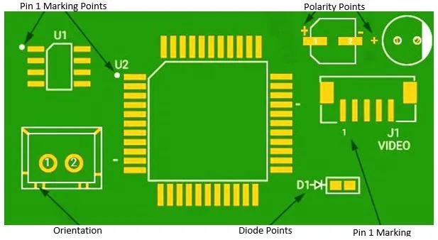
- Orientation Consistency: Align components in the same direction whenever possible to simplify the soldering process. For example, orient all diodes with the cathode marking on the same side to avoid confusion.
By following these guidelines, you can create a layout that not only works electrically but is also easy to manufacture. Always double-check your placement against design rules in your PCB software to catch potential issues early.
Step 3: Designing for Reflow Soldering SMD Components
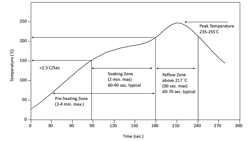
Reflow soldering is the most common method for attaching SMD components to a PCB. It involves applying solder paste to the pads, placing components, and heating the board in a reflow oven to melt the solder and form strong connections. Proper design considerations can make reflow soldering more reliable and reduce defects like cold joints or tombstoning.
First, ensure your solder paste stencil is designed correctly. The stencil openings should match the pad sizes on your PCB, typically with a 1:1 ratio for most components. For finer pitch components (below 0.5 mm), reduce the stencil aperture by about 10% to prevent excess solder paste, which can cause bridging.
Next, consider the reflow profile, which is the temperature curve used during soldering. A typical profile includes four stages: preheat (to 150°C over 60-90 seconds), soak (holding at 150-180°C for 60-120 seconds), reflow (peaking at 235-250°C for 20-40 seconds), and cooling. These values can vary based on the solder paste type, so always refer to the paste manufacturer's recommendations. For lead-free solder, the peak temperature might reach 245°C to ensure proper melting.
During layout design, avoid placing large components next to small ones in the same reflow zone. Larger components can create a thermal shadow, preventing smaller parts from reaching the necessary temperature. If unavoidable, consider adding thermal reliefs or extra vias to balance heat distribution.
Finally, inspect your board after reflow soldering. Look for issues like misaligned components or insufficient solder. If defects occur, adjust your stencil design or reflow profile for the next batch.
Step 4: Key Tips for Optimizing SMD PCB Design
Beyond the basics of footprint creation, component placement, and reflow soldering, there are additional strategies to optimize your SMD PCB design for performance and reliability. Here are some practical tips to consider:
- Use Design Rule Checks (DRC): Most PCB design software includes DRC tools to verify spacing, trace widths, and other parameters. Set your DRC to enforce a minimum trace width of 0.15 mm for standard signals and 0.3 mm for power traces to handle currents up to 1A safely.
- Minimize Via Usage: While vias are necessary for multi-layer boards, excessive vias can weaken the board structure and increase manufacturing costs. Aim to keep vias under 10% of your total trace length in high-density areas.
- Plan for Test Points: Add test points for critical signals or power lines to simplify debugging after assembly. A test point pad of 1 mm diameter is usually sufficient for most probes.
- Account for Panelization: If producing multiple boards, design with panelization in mind. Leave at least 2 mm of clearance between individual boards in a panel to allow for clean separation during depanelization.
These small adjustments can significantly improve the quality of your SMD PCB design, making it easier to manufacture and more robust in real-world applications.
Step 5: Common Mistakes to Avoid in SMD PCB Design
Even with careful planning, mistakes can happen during SMD PCB design. Being aware of common pitfalls can help you avoid costly errors. Here are some issues to watch out for:
- Incorrect Footprints: Always double-check footprint dimensions against the component datasheet. A mismatch as small as 0.1 mm can prevent proper soldering.
- Insufficient Spacing: Crowding components too closely can lead to soldering defects or interference. Maintain at least 0.3 mm spacing for fine-pitch components.
- Poor Thermal Design: Neglecting heat dissipation can cause components to overheat. For a component dissipating 1W of heat, ensure at least 10 mm2 of copper area or thermal vias for cooling.
- Ignoring Manufacturer Guidelines: Each assembly house may have specific design rules for solder paste stencils or reflow profiles. Review their requirements before finalizing your design.
By staying vigilant and reviewing your design at every stage, you can minimize these risks and produce a high-quality SMD PCB.
Step 6: Tools and Resources for SMD PCB Design
Having the right tools can streamline your SMD PCB design process. Many software options are available that cater to both beginners and professionals. Look for platforms that offer built-in libraries for SMD components, DRC features, and 3D visualization to preview your design.
Additionally, online resources like component datasheets, design guides, and community forums can provide valuable insights. Some manufacturers also offer free stencil design tools or reflow profile calculators to assist with soldering preparation.
Invest time in learning your chosen tools thoroughly. Familiarity with shortcuts and advanced features can save hours during the design process, especially for complex SMD layouts.
Conclusion: Take Your SMD PCB Design Skills to the Next Level
Mastering SMD PCB design is a journey that combines technical knowledge with practical experience. By focusing on accurate footprint creation, strategic component placement, and optimized reflow soldering techniques, you can create reliable and efficient PCBs for any project. Remember to leverage design tools, adhere to best practices, and continuously refine your skills with each board you design.
Whether you're working on a small prototype or a large-scale production run, the principles covered in this SMD PCB design tutorial will serve as a solid foundation. Start applying these tips to your next project, and watch as your designs become more professional and effective.
With dedication and attention to detail, you'll soon be crafting high-quality SMD PCBs that meet the demands of modern electronics. Keep learning, keep designing, and let your creativity shine through every board you build.


