 ALLPCB


As an electrical engineer designing a PCB, one of the most critical decisions you’ll face is choosing the right power supply solution. Should you use a Low Dropout (LDO) regulator or a switching regulator? This choice impacts efficiency, noise, cost, and overall performance of your design. In this guide, we’ll break down the key differences between LDOs and switching regulators, focusing on PCB design considerations, efficiency, EMI challenges, and a step-by-step power supply selection guide. Whether you’re optimizing for “LDO vs switching regulator PCB design” or tackling “switching regulator EMI considerations,” this post will help you make an informed decision.
Quick Answer: LDO vs. Switching Regulator – Which Should You Choose?
For a quick decision: Use an LDO regulator if your PCB design prioritizes low noise, simplicity, and small voltage drops (e.g., powering noise-sensitive analog circuits). Choose a switching regulator if efficiency and power handling are critical, especially for battery-powered or high-current applications, but be prepared to address electromagnetic interference (EMI). Dive into the detailed sections below for a deeper understanding of “LDO regulator efficiency PCB” challenges and more.
Introduction: Why Power Supply Choice Matters in PCB Design
Power supply design is the backbone of any PCB. A poorly chosen regulator can lead to inefficiencies, overheating, or even system failures due to noise or EMI. LDO and switching regulators are the two primary options for voltage regulation, each with unique strengths and trade-offs. As engineers, we often face constraints like space, cost, and performance requirements. Understanding the nuances of “LDO vs switching regulator PCB design” is essential to meeting these demands. This guide will walk you through the technical details, practical tips, and real-world considerations to ensure your power supply aligns with your project’s needs.
What Are LDO and Switching Regulators? A Technical Overview
Low Dropout (LDO) Regulators
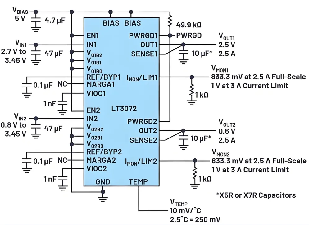
An LDO regulator is a type of linear regulator that maintains a stable output voltage with a very small difference between input and output voltage (dropout voltage), often as low as 0.1V to 0.5V. LDOs are simple to implement, requiring minimal external components—typically just input and output capacitors. They work by dissipating excess voltage as heat, which makes them less efficient at high current or large voltage drops but ideal for low-noise applications.
Key Specs Example: A common LDO like the Texas Instruments TPS7A47 can handle an input voltage range of 3V to 36V, with a dropout voltage of 0.307V at 1A, and offers ultra-low noise (4.17 μVrms) for sensitive circuits.
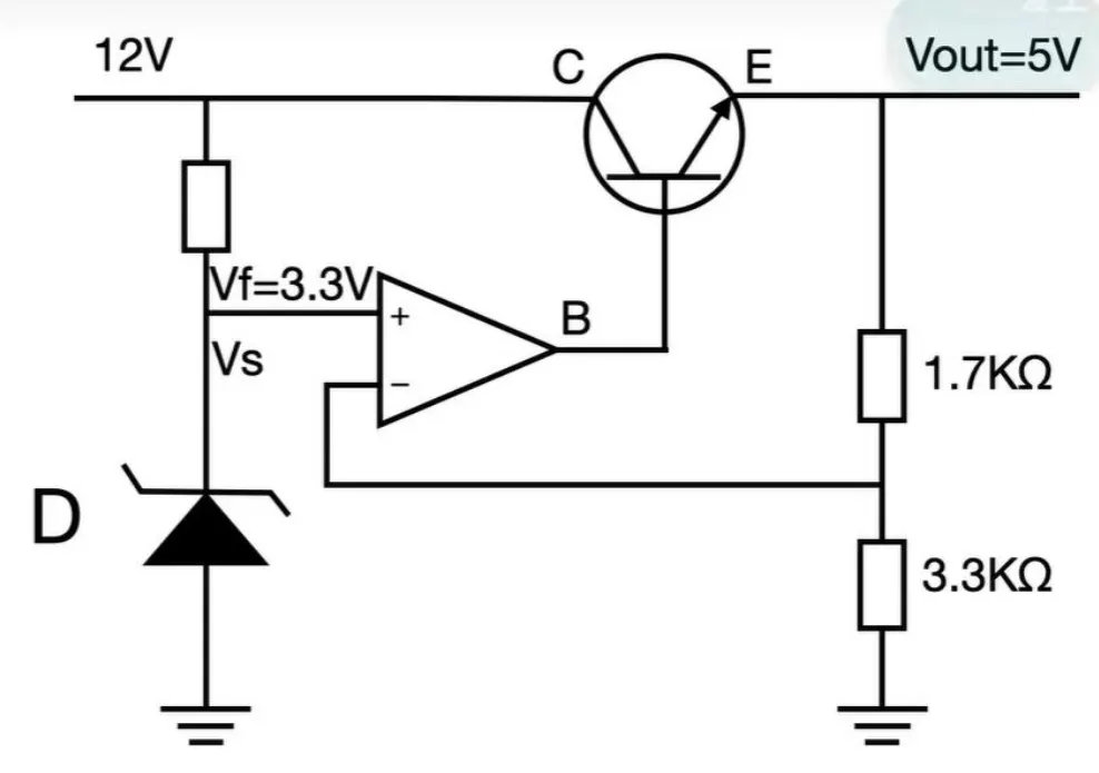
Switching Regulators
Switching regulators, often referred to as DC-DC converters (buck, boost, or buck-boost), use a switching mechanism to convert input voltage to the desired output. They operate by rapidly turning a transistor on and off, storing energy in inductors or capacitors, which results in much higher efficiency—often 80-95% compared to LDOs. However, this switching action introduces noise and EMI, requiring careful PCB design and additional components like inductors and filters.
Key Specs Example: The Texas Instruments LM2675, a buck switching regulator, supports an input voltage of 8V to 40V, outputs 1.2V to 37V at up to 1A, and achieves up to 92% efficiency, but requires careful layout to minimize EMI.
Suggested Image Placement: Insert a diagram here illustrating the internal working of an LDO (linear dissipation) versus a switching regulator (PWM switching). ALT Text: “LDO vs Switching Regulator Working Principle Diagram”
Comparing LDO vs. Switching Regulators: Key Factors for PCB Design
Let’s dive into the critical aspects of “LDO vs switching regulator PCB design” by comparing their performance across efficiency, noise, size, cost, and thermal management.
1. Efficiency: LDO Regulator Efficiency PCB Challenges
LDO Efficiency: LDOs are inherently inefficient because they dissipate excess voltage as heat. Efficiency can be calculated as (Vout / Vin) × 100%. For example, if Vin = 5V and Vout = 3.3V, efficiency is only 66%. At higher currents (e.g., 1A), this inefficiency leads to significant power loss (1.7W in this case), requiring heat sinks or larger PCB areas for thermal dissipation.
Switching Regulator Efficiency: Switching regulators shine here, often achieving 85-95% efficiency. For the same 5V to 3.3V conversion at 1A, a switching regulator might waste only 0.3W, reducing thermal stress and extending battery life in portable devices.
Takeaway for Engineers: If power efficiency is a priority (e.g., in battery-powered IoT devices), a switching regulator is the better choice. For low-power, noise-sensitive designs like audio amplifiers, prioritize an LDO despite “LDO regulator efficiency PCB” challenges.
2. Noise and EMI: Switching Regulator EMI Considerations
LDO Noise: LDOs produce very little noise since they operate linearly without switching. Their output ripple is often in the microvolt range (e.g., 10 μVrms for high-performance LDOs), making them ideal for analog circuits, RF modules, or precision sensors.
Switching Regulator EMI: Switching regulators generate significant EMI due to high-frequency switching (typically 100 kHz to several MHz). This can interfere with nearby circuits, especially in mixed-signal designs. “Switching regulator EMI considerations” include using proper shielding, ground planes, and filters. For instance, placing a ferrite bead and capacitor near the output can reduce ripple from 50 mVpp to under 10 mVpp.
Takeaway for Engineers: If your PCB includes noise-sensitive components, an LDO is safer. For switching regulators, dedicate time to EMI mitigation strategies during layout (more on this later).
3. Size and Component Count
LDO Size: LDOs require fewer components—often just two capacitors—leading to a smaller PCB footprint. This simplicity is a boon for space-constrained designs like wearables.
Switching Regulator Size: Switching regulators need inductors, diodes, and additional capacitors, increasing the footprint. For example, a buck converter might require a 10 μH inductor and multiple ceramic capacitors, occupying 2-3 times the space of an LDO.
Takeaway for Engineers: Choose an LDO for compact designs; opt for a switching regulator if space isn’t a primary constraint and efficiency matters more.
4. Cost
LDO Cost: LDOs are generally cheaper, with prices ranging from $0.50 to $2 for common models. Their minimal external components keep BOM costs low.
Switching Regulator Cost: Switching regulators cost more—often $1 to $5 per IC—plus the expense of inductors and capacitors, potentially doubling the total cost.
Takeaway for Engineers: Budget-conscious projects favor LDOs, while high-performance designs may justify the cost of switching regulators.
Power Supply Selection Guide for PCB Engineers
Choosing the right regulator for your PCB isn’t a one-size-fits-all decision. Follow this “power supply selection guide PCB” framework to align your choice with project requirements.
Step 1: Define Power Requirements
Start by identifying your input voltage (Vin), output voltage (Vout), and current draw (Iout). For example, powering a microcontroller at 3.3V, 500 mA from a 12V source suggests a large voltage drop—favoring a switching regulator for efficiency.
Step 2: Assess Noise Sensitivity
Determine if your circuit is noise-sensitive. Analog-to-digital converters (ADCs) or RF circuits often require clean power, making LDOs the safer bet. If noise isn’t a concern (e.g., digital logic), a switching regulator works fine with proper filtering.
Step 3: Evaluate Efficiency Needs
Calculate potential power loss. For Vin = 12V, Vout = 3.3V, Iout = 500 mA, an LDO would dissipate (12V - 3.3V) × 0.5A = 4.35W as heat. A switching regulator at 90% efficiency loses only about 0.48W—a huge difference for battery life.
Step 4: Consider PCB Space and Budget
Check available board space and cost constraints. If your design is cramped or budget-tight, an LDO’s simplicity might outweigh efficiency losses.
Step 5: Plan for EMI Mitigation (If Using Switching Regulators)
For switching regulators, allocate space for EMI filters and follow layout best practices (discussed next). If EMI risks are high and mitigation isn’t feasible, revert to an LDO.
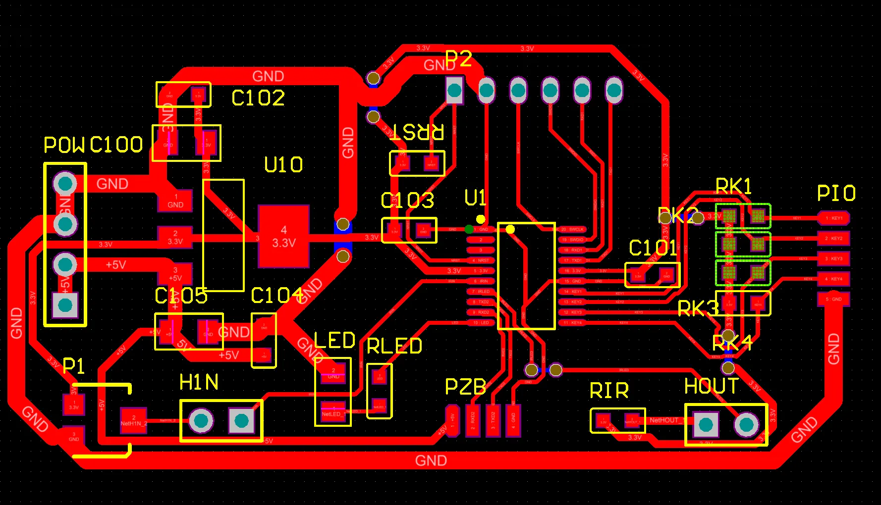
PCB Layout Tips for LDO and Switching Regulators
LDO Layout Tips
- Place Capacitors Close: Position input and output capacitors as close as possible to the LDO pins to minimize noise. Use ceramic capacitors with low ESR (e.g., 0.01 ohms) for stability.
- Thermal Management: Ensure adequate copper area or vias under the LDO for heat dissipation, especially at high currents. For a 1W dissipation, a 2 cm2 copper pad can help keep temperatures below 85°C.
Switching Regulator Layout Tips (EMI Focus)
Given the “switching regulator EMI considerations,” layout is critical to minimize interference.
- Shorten High-Current Loops: Keep the switching node (where the inductor connects) as short as possible to reduce radiated EMI. A loop area under 1 cm2 is ideal.
- Ground Plane: Use a solid ground plane under the switching regulator to provide a low-impedance return path. Avoid splitting the ground plane near the regulator.
- Filter Components: Place a ferrite bead and output capacitor near the load to suppress high-frequency noise. For a 1 MHz switching frequency, a 600-ohm ferrite bead can attenuate noise by 20 dB.
Real-World Applications: When to Use LDO vs. Switching Regulators
LDO Use Cases
- Analog Circuits: Powering op-amps or ADCs where noise must be below 50 μVrms.
- Low-Power Devices: Small sensors drawing under 100 mA, where efficiency loss is negligible.
Switching Regulator Use Cases
- Battery-Powered Systems: IoT devices or drones needing high efficiency to maximize runtime.
- High-Current Loads: Powering microcontrollers or LEDs at 1A or more, where LDO heat dissipation is impractical.
Common Pitfalls and How to Avoid Them
LDO Pitfall: Underestimating heat dissipation. Always calculate power loss and verify thermal limits. Use a heatsink if dissipation exceeds 0.5W.
Switching Regulator Pitfall: Ignoring EMI. Failing to follow layout guidelines can cause certification failures. Test early with an EMI probe to identify problem areas.
Conclusion: Making the Right Choice for Your PCB Power Needs
Choosing between an LDO and a switching regulator for your PCB design boils down to balancing efficiency, noise, cost, and space. LDOs are your go-to for low-noise, simple designs despite “LDO regulator efficiency PCB” drawbacks. Switching regulators excel in efficiency and power handling but demand attention to “switching regulator EMI considerations.” Use the “power supply selection guide PCB” steps outlined above to align your decision with project goals. By understanding the trade-offs and applying best practices in “LDO vs switching regulator PCB design,” you’ll ensure a robust, reliable power solution for your next project.
Have a specific design challenge or question about regulators? Drop a comment below, and let’s discuss! For further reading, explore resources like Texas Instruments’ application notes or Analog Devices’ design tools to deepen your knowledge.


