 ALLPCB


Introduction
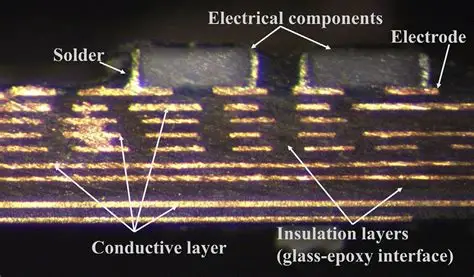
Thin printed circuit boards, typically under 0.8 mm in total thickness, enable compact electronics in applications like wearables, medical devices, and IoT modules. Designing these boards demands precise thin PCB design rules to balance high density with reliable production. Manufacturers face unique challenges such as increased warpage risk and handling fragility, making design for manufacturability thin PCB a critical focus. Engineers must optimize PCB layout thin from the outset to avoid costly rework or failures. This article explores structured guidelines drawn from established industry practices, ensuring layouts support fabrication tolerances and assembly success. By adhering to these principles, designers achieve higher yields and performance in miniaturized systems.
What Are Thin PCBs and Why Thin PCB Design Rules Matter
Thin PCBs refer to rigid boards with finished thicknesses from 0.2 mm to 0.8 mm, often using thin cores and minimal prepreg buildup. These boards support fine-pitch components and high-layer counts in limited spaces, driving demand in consumer and automotive sectors. However, reduced material volume amplifies stresses during lamination, etching, and reflow, leading to defects like delamination or misalignment. Thin PCB design rules address these by specifying layout constraints that align with fabrication capabilities. Ignoring them results in lower yields, as thin substrates deform more under thermal cycling. For electric engineers, mastering these rules ensures signal integrity and mechanical stability in high-density interconnects.
The relevance intensifies with shrinking device footprints, where standard 1.6 mm boards prove impractical. Optimized thin PCB design rules minimize risks like trace shorts from warpage or via failures from drill wander. They promote symmetry in copper distribution and layer buildup, foundational to manufacturability. Engineers benefit from proactive DfM checks, reducing iteration cycles. Ultimately, these rules transform conceptual layouts into producible hardware.
Key Technical Principles in Thin PCB Layout
Trace Width and Current Handling
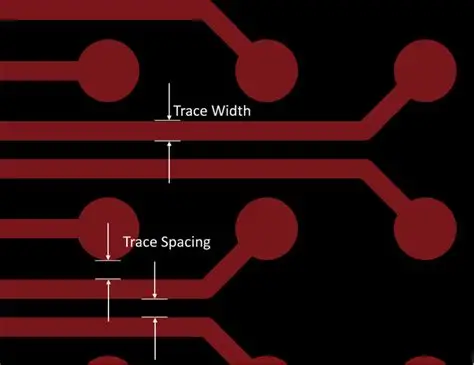
Minimum trace width thin PCB starts with fabrication limits, typically around 0.1 mm for advanced processes, but engineers calculate based on current, temperature rise, and copper weight. Thinner boards use lighter copper foils, like 1 oz/ft2, which demand wider traces for equivalent ampacity to prevent overheating. IPC-2221 provides generic guidelines for sizing, emphasizing external traces need more width due to poorer heat dissipation in thin stacks. Overly narrow traces etch unevenly on thin substrates, risking opens or high resistance. Balancing density with reliability requires iterative simulation of thermal profiles during layout.
In practice, power traces on thin PCBs should exceed signal lines by factors of 2-3 times width, depending on load. This prevents hotspots that exacerbate warpage through localized expansion. Engineers verify widths against layer position, as inner traces benefit from surrounding dielectrics for cooling.
Minimum Spacing for Isolation and Yield
Minimum spacing thin PCB follows voltage levels and density goals, with 0.1 mm as a common baseline for low-voltage signals. Closer spacing risks arcing or crosstalk, amplified in thin boards where fields concentrate due to proximity to planes. IPC-2221 outlines spacing tables scaling with voltage, recommending creepage margins for uncoated boards. In high-density zones, maintain at least 3:1 width-to-spacing ratios to aid etching uniformity. Thin layouts demand vigilant DRC checks to avoid bridging during solder mask application.
Environmental factors like humidity influence spacing needs, as thin boards absorb moisture faster. Engineers incorporate test coupons for spacing verification in panels.
Via and Hole Design Constraints
Vias in thin PCBs benefit from low aspect ratios, under 1:1 drill-to-board thickness, easing plating. Minimum via diameters scale to 0.15 mm finished, with annular rings at least 0.1 mm to withstand registration tolerances. Staggered via fields prevent breakout on thin edges, while filled vias enhance rigidity. Blind or buried vias suit multilayer thin stacks, reducing surface clutter. Overuse strains thin cores during sequential lamination.
Pad-to-via spacing mirrors trace rules, ensuring solder joint integrity. Engineers prioritize via tents in solder mask for contamination protection.
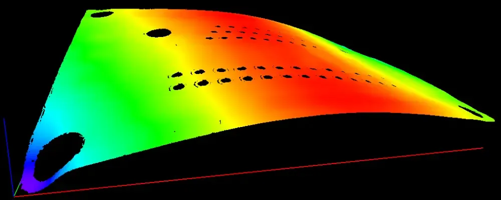
Warpage Control Mechanisms
Warpage dominates thin PCB challenges, as asymmetric stresses bow boards beyond acceptable limits. Symmetric stackups, with mirrored copper and dielectric thicknesses, counter lamination shrinkage differentials. Copper balancing distributes mass evenly, minimizing gradients from heavy ground planes. IPC-6012 sets bow and twist limits at 0.75% for surface-mount assemblies over critical dimensions. Routing patterns avoid large unpopulated areas, which warp freely.
Thermal management integrates balanced trace routings to equalize CTE mismatches. Fixtures during reflow hold thin panels flat.
Best Practices for Design for Manufacturability in Thin PCBs
Start with symmetric multilayer stackups, pairing thin cores like 0.1 mm with equal prepregs on both sides. This aligns with DfM principles for uniform curing pressures. Panelize singles on carriers with breakaway tabs, adding V-scoring or mouse bites for clean separation. Place three fiducials per panel corner, oversized at 1 mm, for optical alignment.
Route traces perpendicular to board edges in border zones to prevent delamination. Minimum 5 mm clearance from edges for components avoids handling damage. Chamfer corners at 45 degrees, reducing stress risers. For high-density, use teardrops on pads to distribute etch currents evenly.
Incorporate test points with 0.5 mm pads, spaced 1 mm minimum, for in-circuit probing without shorts. Simulate warpage via FEA tools, targeting under 0.5% proactively. Collaborate early with fabricators on capabilities, specifying thin PCB design rules in fab drawings.
- Stackup: Symmetric layers — Reduces bow from shrinkage
- Traces: 0.1 mm min width/space — Etch yield, signal integrity
- Vias: 0.15 mm min drill — Plating uniformity
- Panel: Carrier with fiducials — Handling, registration
- Edges: 5 mm setback, chamfers — Mechanical stability
Troubleshooting Common Thin PCB Layout Issues
Engineers often encounter warpage exceeding IPC-A-600 acceptability after assembly. Root causes include asymmetric copper or oversized cutouts; remedies involve balancing pours and adding stiffeners. Trace bridging arises from insufficient spacing in humid processes, resolved by widening gaps or enhancing mask registration. Via cracks signal drill misalignment, mitigated by pilot holes or laser drilling.
A typical case: A 0.4 mm 4-layer board warped 1.2% due to unbalanced ground plane. Redesign with symmetric fills and panel supports dropped it to 0.4%, passing qualification. Iterative DfM reviews catch these pre-prototype.
Conclusion
Thin PCB design rules form the backbone of reliable, high-yield layouts in compact electronics. Optimizing PCB layout thin through trace sizing, spacing, and symmetry directly enhances manufacturability. Key to success lies in proactive warpage control and panelization strategies. Electric engineers applying these structured principles minimize defects while maximizing density. Future designs will lean heavier on these rules as devices thin further, ensuring robust performance.
FAQs
Q1: What are the primary thin PCB design rules for minimum trace width thin PCB?
A1: Minimum trace width thin PCB aligns with fabrication capabilities, often 0.1 mm, sized per current using standard guidelines. Wider traces suit power paths to manage heat in thin stacks. Verify against layer and copper weight for thermal rise under 20°C. This ensures etch reliability and signal fidelity in dense layouts.
Q2: How does minimum spacing thin PCB impact design for manufacturability thin PCB?
A2: Minimum spacing thin PCB, starting at 0.1 mm for low voltage, prevents shorts and crosstalk while aiding mask alignment. Scale up for higher voltages per established tables. Proper spacing boosts yield by 10-20% in thin boards prone to deformation. Integrate into DRC for automated checks.
Q3: Why is warpage control essential in PCB layout thin?
A3: Warpage in PCB layout thin exceeds limits faster due to low rigidity, risking component shifts in reflow. Symmetric designs keep it under 0.75% per standards. Balance copper and use carriers to stabilize. This upholds assembly precision in miniaturized products.
Q4: What stackup strategies improve thin PCB design rules adherence?
A4: Symmetric stackups with matched dielectrics minimize CTE-induced bow in thin PCB design rules. Thin cores pair with minimal prepregs for uniformity. Simulate for validation. These practices enhance overall manufacturability and reliability.
References
IPC-2221B — Generic Standard on Printed Board Design. IPC, 2009
IPC-6012E — Qualification and Performance Specification for Rigid Printed Boards. IPC, 2017
IPC-A-600K — Acceptability of Printed Boards. IPC, 2020


