 ALLPCB


Choosing the Right Connectors for High-Frequency 5G PCBs
High-frequency 5G printed circuit boards demand connectors that preserve signal integrity across millimeter-wave frequencies. Engineers must evaluate connector performance at the system level because even small mismatches introduce reflections that degrade overall network throughput. The selection process begins with understanding the operating frequency band, required power handling, and environmental conditions the assembly will encounter. Proper connector choice directly influences insertion loss, return loss, and phase stability throughout the product lifecycle.
Why Connector Selection Matters in 5G Systems
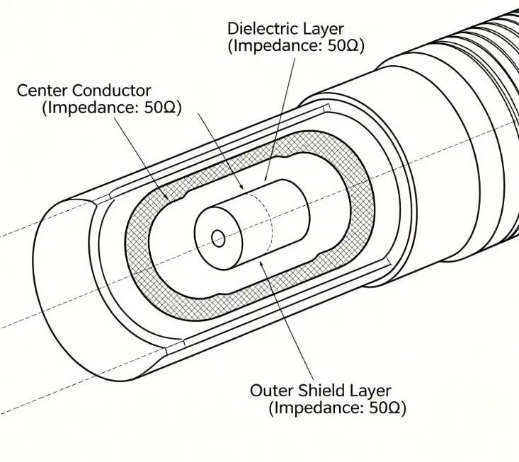
5G PCB connectors operate in environments where frequencies extend well into the millimeter-wave range. At these frequencies, traditional interconnects that function adequately at lower bands exhibit unacceptable attenuation and distortion. High frequency connectors must maintain consistent characteristic impedance, typically 50 ohms, to prevent standing waves that reduce transmitted power. RF connectors designed for mmWave applications incorporate precision-machined interfaces and low-loss dielectric materials that minimize skin-effect losses. When connector impedance matching is neglected, the resulting voltage standing wave ratio rises sharply, limiting the effective range and data rate of the radio unit.
Signal propagation at millimeter-wave frequencies occurs predominantly along the surface of conductors, making surface finish and geometry critical. The connector body and center contact must form a continuous coaxial structure that matches the transmission-line impedance of the PCB trace or stripline. Any abrupt change in diameter or dielectric constant creates a discontinuity that reflects part of the incident wave. Engineers therefore examine the connector’s specified maximum operating frequency, typical insertion loss per mated pair, and voltage standing wave ratio across the target band. Mechanical tolerances also affect performance; even a few micrometers of misalignment can shift the effective impedance outside acceptable limits.
Thermal expansion differences between the connector housing and the PCB substrate introduce additional variables. Materials with matched coefficients of thermal expansion reduce stress on solder joints during temperature cycling. Plating thickness and composition further influence both electrical conductivity and long-term reliability under humidity and vibration. These interrelated factors require a systematic evaluation rather than selection based solely on form factor.
Best Practices for Selecting 5G PCB Connectors
Begin the selection process by defining the exact frequency range, power level, and number of mating cycles expected in service. Compare candidate connectors against these parameters using manufacturer-supplied S-parameter data rather than relying on nominal specifications alone. Verify that the connector footprint on the PCB maintains the required ground plane clearance and via stitching to support the intended characteristic impedance. When multiple connector families satisfy the electrical requirements, evaluate mechanical robustness, ease of automated assembly, and availability of compatible cable assemblies.
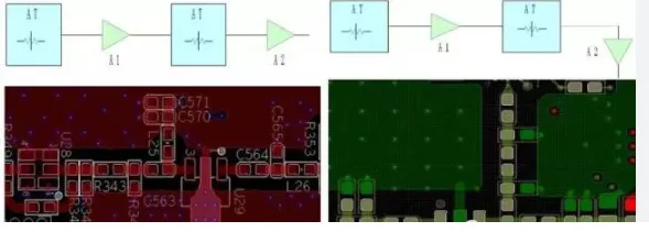
During layout, maintain a smooth transition from the PCB trace to the connector launch. Use tapered ground pours and appropriately sized antipads to control the local impedance. After assembly, perform time-domain reflectometry or vector network analyzer measurements on representative samples to confirm that connector impedance matching meets design targets. These measurements also reveal any process-related defects such as excess solder or misaligned center contacts.
Assembly and Quality Considerations
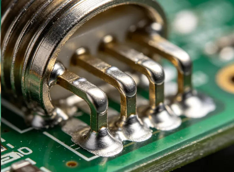
Connector installation on high-frequency boards follows established soldering and inspection practices. Controlled reflow profiles prevent excessive heating that could degrade the connector’s dielectric or plating. Post-assembly inspection focuses on solder fillet geometry, center-contact alignment, and absence of flux residue that could affect high-frequency performance. When boards undergo environmental stress screening, connectors are monitored for changes in return loss and insertion loss to detect latent defects.
Conclusion
Selecting suitable connectors for high-frequency 5G PCBs requires balancing electrical performance, mechanical durability, and manufacturing repeatability. Engineers who evaluate impedance continuity, frequency response, and assembly compatibility early in the design cycle reduce the risk of costly respins. Consistent application of these principles supports reliable operation across the demanding millimeter-wave spectrum.
FAQs
Q1: What characteristics define suitable 5G PCB connectors for millimeter-wave applications?
A1: Suitable 5G PCB connectors maintain 50-ohm impedance, exhibit low insertion loss, and support the target frequency band with acceptable voltage standing wave ratio. They incorporate precision interfaces and low-loss dielectrics that preserve signal integrity when properly matched to the PCB launch structure.
Q2: How does connector impedance matching affect 5G radio performance?
A2: Connector impedance matching minimizes reflections that would otherwise reduce transmitted power and introduce phase distortion. Poor matching raises return loss, which directly limits the effective isotropic radiated power and receiver sensitivity of the 5G module.
Q3: Which industry standards guide the qualification of high-frequency connectors on PCBs?
A3: IPC-6012E establishes qualification and performance requirements for rigid printed boards that host RF connectors. J-STD-001H defines soldering requirements that ensure reliable electrical and mechanical connections at the connector-to-board interface.
Q4: What practical steps help verify connector performance after assembly?
A4: Engineers perform vector network analyzer measurements on assembled boards to confirm insertion loss and return loss across the operating band. Time-domain reflectometry further identifies any impedance discontinuities introduced during the connector mounting process.
References
IPC-6012E — Qualification and Performance Specification for Rigid Printed Boards. IPC, 2017
J-STD-001H — Requirements for Soldered Electrical and Electronic Assemblies. IPC, 2020
IEC 61169-1 — Radio-frequency connectors — Part 1: Generic specification. IEC, 2019





